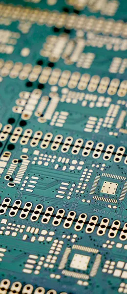
PCBs (Printed Circuit Boards) are key components in electronic devices, consisting of multiple elements such as an insulating substrate, printed conductors, and pads. This article will take an in-depth look at these elements, providing a detailed explanation of each—from the selection of the insulating substrate to the design of printed conductors and the quality inspection of printed circuit boards.

Advanced: A Complete List of Components in a PCB
"Insulating substrate + printed conductors + pads" are the three core elements, but finished circuit boards also contain several other equally essential components:
| Composition | Function | Common Forms |
|---|---|---|
| Insulating Substrate | Provides mechanical support and electrical insulation | FR-4, CEM Series, Polyimide, Ceramic |
| Copper Foil Circuit | Electrical Conductivity and Signal Transmission | Electrolytic copper foil, rolled copper foil |
| Solder pad | Component Soldering and Electrical Connections | Surface-mount pads, through-hole pads, BGA ball grids |
| Via | Interlayer Interconnects | Through-holes, blind holes, buried holes, microvias |
| Solder Mask | Prevents solder from adhering to non-soldered areas and prevents oxidation | Green and Other Colored Photosensitive Inks |
| Screen-printed layer | Label Part Numbers and Directions | White or other-colored characters |
| Surface Treatment | Protects the pads and ensures solderability | Solder-plated, electroless gold, OSP, gold-plated |
| Markings and Process Edges | Optical Alignment, Panel Joining, and Assembly | Marking points, machining edges, and locating holes |
- The first three items determine the electrical functionality.: The substrate, circuit traces, and pads constitute the basic capabilities of a circuit board;
- The last five items determine manufacturability: Solder mask, screen printing, surface treatment, and other processes determine whether the board can be assembled successfully;
- If any one of these is missing, problems will arise.: For example, missing Mark points can prevent the component from being positioned correctly.

For copper foil specifications, seeCopper Foil: The Lifeline of PCBs; For information on copper-clad laminate materials, seePCB Materials。
Insulating Substrates: Material Selection Determines Quality
Insulating substrates form the foundation of PCBs and are primarily divided into two categories: organic substrate materials and inorganic substrate materials. Organic substrate materials use reinforcing materials such as glass fiber. After being impregnated with a resin binder and dried, they are coated with copper foil and processed under high temperature and pressure. These substrates are known as copper-clad laminates (CCL), commonly abbreviated asCopper-Clad Laminate. It is the primary material used in PCBs.
Inorganic substrate materials primarily include ceramic substrates and steel substrates coated with ceramic glaze. Ceramic substrates are mainly composed of 96% alumina and are typically used in hybrid integrated circuits and multi-chip microassembly circuits. They are characterized by high-temperature resistance, a smooth surface, and high chemical stability. In contrast, enamel-coated steel substrates overcome the limitations of ceramic substrates—such as size constraints and high dielectric constant—and are commonly used in the manufacture of high-speed circuits, making them suitable for certain digital products.
Advanced: How to Choose Between Organic and Inorganic Substrates
| Category | Representative Materials | Advantages | Limitations | Typical Applications |
|---|---|---|---|---|
| Organic | FR-4, CEM-1/CEM-3 | Low cost and good workability | Poor thermal conductivity; limited temperature resistance | General Electronics |
| Organic (Flexible) | Polyimide (PI) | Flexible and heat-resistant | High cost, poor dimensional stability | FPC, Rigid-Flex |
| Inorganic | Ceramics (alumina, etc.) | High thermal conductivity and good insulation | Brittle, limited in size, expensive | High Power, High Frequency |
| Inorganic | Ceramic-Coated Steel | Can be made larger; has a lower dielectric constant | Unique Process | High-speed circuits, certain digital products |
| Metal-based | Aluminum-based, copper-based | Good thermal conductivity | Mostly single-sided | LEDs, Power Modules |
The typical order of selection is:Start with FR-4; if thermal conductivity is insufficient, use a metal substrate; only switch to ceramic if performance is inadequate or the heat flux density is extremely high.. The cost difference is an order of magnitude, so there's no need to choose the most expensive option right from the start.
- Check the temperature resistance: For lead-free processes and high-power applications, the Tg must be increased;
- Check the frequency: GHz-level applications require materials with low Df;
- Review the mechanical requirements: Use PI for flexibility, and a metal substrate for strength and heat dissipation.
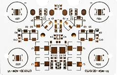
For information on thick copper boards, see8 Things to Keep in Mind When Applying Copper to a PCB; For a comparison of the three types of rigid copper-clad laminates, seeA Comparison of the Properties of the Three Most Common Types of Rigid Copper-Clad Laminates。
Printed Circuit Lines: The Design Must Be Reasonable
Printed conductors are a critical component of PCBs, and their design requires consideration of multiple factors. Generally, wider printed conductors are better able to carry current and are easier to manufacture. In addition, attention must be paid to the peel strength between the copper foil and the substrate.
It is recommended to use printed circuit trace widths of 0.5 mm, 1.0 mm, 1.5 mm, and 2.0 mm. A general design principle is that signal traces should be narrower than power traces, which in turn should be narrower than ground traces. In addition, the spacing between printed traces must be determined comprehensively based on factors such as the substrate material, operating environment, and capacitance distribution; generally, the spacing between traces is equal to the trace width.
To minimize parasitic coupling between wires, they should be routed in the order in which the signal flows. The input and output terminals should be placed as far apart as possible and, ideally, separated by a ground line. Avoid right angles or sharp turns when routing; the path should be smooth.
When connecting SMT pads, printed conductors are generally not designed to connect two pads directly; instead, it is recommended to route them away from both ends before connecting them. To prevent the integrated circuit from warping during reflow soldering, the connecting conductors should, in principle, extend from either end of the pad to maintain balanced solder tension and prevent warping.
Advanced: The Relationship Between Wire Width, Copper Thickness, and Current Carrying Capacity
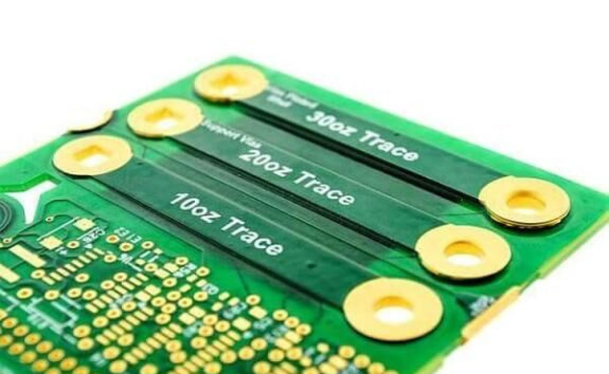
The maximum current a printed conductor can carry depends on itsCross-sectional area, which is the product of the trace width and the copper thickness. When designing, both of these factors must be taken into account, and sufficient margin must be allowed:
| Copper Thickness | Approximate current-carrying capacity for a 1 mm wire width | Applicable |
|---|---|---|
| 1 oz (35 μm) | Approx. 1–2 A | Signals and Low-Power Power Supply |
| 2 oz (70 μm) | Approximately 2–3 A | Universal Power Rail |
| 3 oz (105 μm) | Approximately 3–5 A | Power Modules, Motor Drives |
| 4–6 oz | 5 A or higher | High-Current Busbars, Automotive Electronics |
The values in the table are for reference only; actual values may vary by as much as several times, depending on factors such as temperature rise requirements, whether the traces are routed on inner or outer layers, and whether there is copper plating around them for heat dissipation. Therefore,Critical power lines should be accounted for separately....you can't just rely on a generic form.
- Determine the Maximum Continuous Current, using peak operating conditions and allowing for a margin;
- Determine the Allowable Temperature Rise, typically 10 °C or 20 °C;
- Consult the table to determine the required cross-sectional area, Note the differences between the inner and outer layers;
- Calculating Line Width or Copper Thickness from Cross-Sectional Area;
- Verify Via Placement, The flow capacity at the transition point must be verified separately.
See "Choosing Between Board Thickness and Copper Thickness"Board Thickness and Copper Thickness in PCB Design; For the causes of copper strip detachment, seeThree Causes of Copper Strip Delamination on PCBs。
PCB Quality Inspection: Ensuring Reliability
The quality of PCBs directly affects the performance and reliability of electronic devices. Quality inspection is a critical step in the manufacturing process. The following are some commonly used inspection methods:
- Visual Inspection: Inspect surface finish, screen print clarity, and pad condition, among other factors. Conduct a manual inspection to determine whether any defects are present.
- Electrical Performance Testing: This includes measurements of insulation resistance and continuity to ensure the circuit board's insulation and continuity.
- Solderability Testing of Pads: To test the solder's wetting ability on the pads to ensure the quality of the solder joint.
- Copper Foil Adhesion Test: Check the adhesion of the printed conductors and pads to the substrate to ensure they do not peel off.
In terms of quality inspection, visual inspection and electrical performance testing are commonly used methods that can help identify and resolve potential issues in a timely manner, ensuring the high quality of PCBs.
Advanced: Four Key Points in Pad Design
- Size-Matching Packaging: Pad dimensions should be designed according to the values recommended in the device datasheet; if they are too large, misalignment is likely, and if they are too small, cold solder joints may occur;
- There must be sufficient symmetry.: The dimensions of the pads at both ends should be symmetrical relative to the connected copper area; otherwise, the melting times on both sides will differ during reflow, which can easily cause tombstoning;
- Thermal isolation must be done properly: Pads connected to large areas of copper must be patterned; otherwise, heat will be rapidly dissipated during soldering;
- Solder mask openings must be precise: If the opening is too large, it can cause solder bridging; if it is too small, it will limit the solderable area of the pad.
Among these, Rule 3 is most often overlooked in actual design. If one side of a pad is connected to a large copper pour and the other side is connected only to a fine trace, there will be a significant difference in the timing of solder paste melting on the two sides during the reflow process,The surface tension on the side that melts first will pull the device upward....resulting in a "monolith" formation. The solution involves not only implementing thermal isolation but also ensuring that the thermal conditions on both sides of the pad are as consistent as possible.

For pad and surface treatment, seeA Detailed Explanation of the PCB Surface Plating Process; For information on the effects on solderability, seeThe Effect of PCB Via Solderability on Soldering Quality。
PCB circuit boards are a core component of modern electronic devices; they consist of an insulating substrate, printed conductors, and pads, among other elements. Understanding the characteristics and design principles of these elements, as well as the methods for quality inspection, is crucial for ensuring the performance and reliability of electronic devices.
Advanced: A Complete Checklist for Quality Inspection
In addition to the four basic inspections listed in the article, the following inspection steps are typically included in mass production:
- Electrical Testing: Flying-probe or fixture testing to verify network continuity and insulation;
- AOI Inspection: Automatically detect circuit defects, such as notches, copper bulges, and short circuits;
- Impedance Testing: Perform a TDR test on boards with impedance requirements to verify that they fall within the tolerance range;
- Slice Analysis: Copper thickness at the observation window, interlayer adhesion, and dielectric thickness;
- Solderability Testing: Evaluate the solderability of the pads to prevent soldering defects after storage;
- Thermal Stress Testing: Verify the reliability of via metallization under thermal shock.
The combination of these tests depends on the product grade: for consumer products, electrical testing and AOI are typically sufficient, while for automotive and medical products, routine inspections must include cross-section analysis and thermal stress testing.Test items should be commensurate with the cost of product failure....more isn't necessarily better.

For information on quality assessment methods, seeThree Key Metrics for PCB Manufacturing and Methods for Quality Assessment; For HDI manufacturing requirements, see5 Key Requirements in the HDI Manufacturing Process。
Frequently Asked Questions
1. What is a PCB?
A PCB (printed circuit board) is a substrate used to connect and support electronic components. It consists of key elements such as an insulating substrate, printed conductors, and pads, and is a core component of electronic devices.
2. Why choose organic substrate materials?
Organic substrate materials are generally easier to process and less expensive, which is why they are widely used in PCB manufacturing. They offer good insulation and electrical conductivity.
3. Why is quality inspection of PCBs important?
Quality inspection helps identify and resolve potential issues in a timely manner, ensuring the reliability and performance of PCBs. This is crucial for the proper operation of electronic devices.
4. What is the difference between a pad and a via?
Pads are used to solder device leads and serve as the connection interface between the device and the board; vias are used for interlayer interconnections, routing signals from one layer to another. The design rules for the two differ: pad dimensions are determined by the package, while via dimensions are determined by drilling capabilities and the thickness-to-diameter ratio. Through-hole pads combine elements of both and require a specialized via-filling process.
5. Is a thicker solder mask always better?
No. If the solder mask is too thick, it will affect the clarity of the pad openings and may cause assembly interference; if it is too thin, coverage will be inadequate, making it prone to copper exposure in areas with dense circuitry. The standard practice is to ensure the thickness falls within the process specification range and to carefully check whether solder mask bridges are maintained in fine-pitch areas.
6. Does the screen-printed layer affect electrical performance?
Generally not, but there are two points to keep in mind: First, screen printing should not overlap the pads, as this would interfere with soldering; second, in high-frequency circuits, the dielectric properties of the screen-printing ink could theoretically affect surface traces. Although the impact is minimal, it is still recommended to avoid critical RF traces in high-precision applications.
7. How do I choose a surface treatment?
Solder-plated tin is low-cost and offers good solderability, but its flatness is average; electroplated gold provides high flatness and is suitable for fine pitch and multiple reflow cycles, but it is more expensive; OSP is the least expensive option but has a short shelf life. The choice should be based on a comprehensive evaluation of the key component pitch, number of soldering cycles, storage duration, and budget—there is no need to always choose the most expensive option.
8. When is it necessary to mark a point?
Markers are required whenever automatic alignment by a placement machine is needed. Typically, at least two or three markers are placed on each board, distributed diagonally across the board, with blank areas surrounding them—free of solder mask and silkscreen—to ensure proper recognition. When panelizing, panel-level markers must also be placed along the process edges.
9. Why can't right angles be used at the corners of printed circuit traces?
There are two main reasons: First, etching solution tends to pool at right angles, causing over-etching on the outer side and narrowing the line width; second, at high frequencies, right angles can cause impedance discontinuities and radiation. The standard practice is to use 45° chamfers or rounded transitions.
10. Are the “ground planes” on a PCB considered part of the assembly?
Yes. In multilayer boards, the power and ground planes consist of continuous copper foil layers. Although they do not carry signal traces, they serve as return paths, provide shielding, and aid in heat dissipation; as a result, they often have a greater impact on electrical performance than the signal layers. When designing a stack-up, the placement and integrity of these planes are given high priority.
Additional Information:5 Key Requirements and Optimization Strategies for the HDI Manufacturing Process · Chinese-English Glossary of Common Technical Terms Used in Printed Circuit Board Manufacturing