

Thick-Copper PCBs Allow for Sufficient Margin in High-Current Designs
For power conversion, energy storage, and industrial control applications, evaluate copper thickness, lamination, and manufacturing processes while taking into account operating current, allowable temperature rise, and wiring space.

8-Layer Thick Copper PCB · Jingpeng Electronics Product Showcase
3–20 oz
Thickness of the outer copper layer
1–12 oz
Thickness of the inner copper layer
Up to 16 stories
Range of Floors
Design parameters must be evaluated comprehensively in light of board thickness, layout, hole configuration, and material; it cannot be assumed that all limit values can be met simultaneously.
01 / Selection Criteria
As the copper thickness increases, the design must be adjusted accordingly.
This page defines the selection range for thick-copper PCBs as those with trace copper thicknesses of 3 oz or greater. The value of thick copper should be evaluated within the context of a comprehensive electrical and thermal design.
01
Current Path
All other things being equal, increasing the conductor cross-sectional area helps reduce trace resistance; however, the actual current-carrying capacity still depends on the trace width, trace length, and allowable temperature rise.
02
Heat Distribution
Thick copper helps dissipate localized heat, but it cannot replace the design of device heat sinks, interface materials, and the overall airflow path of the device.
03
Manufacturing Match
Increased copper thickness affects etching, resin filling, and solder mask coverage, requiring corresponding adjustments to line width, line spacing, stack-up, and pad design.
Dielectric strength is determined by a combination of factors, including the insulating material, dielectric thickness, clearance, and test conditions; reliability and service life cannot be judged solely based on copper thickness.
02 / Process Capability
Processing Specifications, Centralized Confirmation
The processing specifications listed below are the same as those already provided on this page. Before requesting a quote, please specify the copper thickness and diameter for each layer, the number of layers, and the acceptance criteria. The specific manufacturability will be confirmed through an engineering review.
- Thickness of the outer copper layer
- 3–20 oz (approx. 105–700 μm)
- Thickness of the inner copper layer
- 1–12 oz (approx. 35–420 μm)
- Materials
- FR-4 / High Tg materials, original Tg range: 150–180°C
- Sheet Thickness
- 0.4–5.0 mm
- Number of Floors
- Up to 16 stories
- Minimum finished hole diameter
- 0.3 mm; to be confirmed based on the plate thickness and hole configuration
The conversions between oz and μm are approximate. The thickness of the base copper and finished copper, as well as their tolerances, should be specified in the manufacturing documentation; a high Tg value does not equate to the permissible long-term operating temperature.
03 / Wiring Guide
The thicker the copper, the more important it is to confirm the line width and spacing in advance.
The following are the minimum trace width and spacing references listed on the original page. These are manufacturing parameters; they do not guarantee current-carrying capacity and should not be used directly as design minimums for all projects.
3 oz copper thickness
8 mil
Minimum Line Width / Line Spacing Guidelines
Approximately 0.203 mm
6 oz copper thickness
12 mil
Minimum Line Width / Line Spacing Guidelines
Approximately 0.305 mm
10 oz copper sheet
16 mil
Minimum Line Width / Line Spacing Guidelines
Approximately 0.406 mm
Other cases involving different copper thicknesses, densely spaced pads, or locally narrow traces should be reviewed on a case-by-case basis. Do not simply extrapolate process limits linearly between different copper thicknesses.
04 / Engineering Review
From Current Paths to Assembly: Four Key Points to Verify
01 / Current and Temperature Rise
Specify the continuous current, peak current, duration, ambient temperature, and allowable temperature rise. Traces, vias, connectors, and solder joints should all be included in the current path analysis.
02 / Layering and Copper Distribution
Determine the thickness of the inner and outer copper layers, and evaluate the copper distribution balance, dielectric thickness, and resin fill. When thick copper and fine-pitch areas coexist, first confirm the manufacturing tolerance.
03 / Holes and Pads
Determine the finished hole size, copper fill, and connection method based on the board thickness. When connecting large copper pads, it is also important to balance current requirements with the heat absorbed during soldering.
04 / Solder Mask Application and Inspection
Confirm the thick copper sidewall coverage, solder mask openings, and assembly requirements. For dielectric strength, insulation, and soldering heat resistance tests, specify the methods, conditions, and acceptance criteria.
05 / Product Showcase
Thick-Copper PCB Products and Applications

10-layer thick copper backplane
Pay attention to power distribution, connector areas, and board thickness coordination.
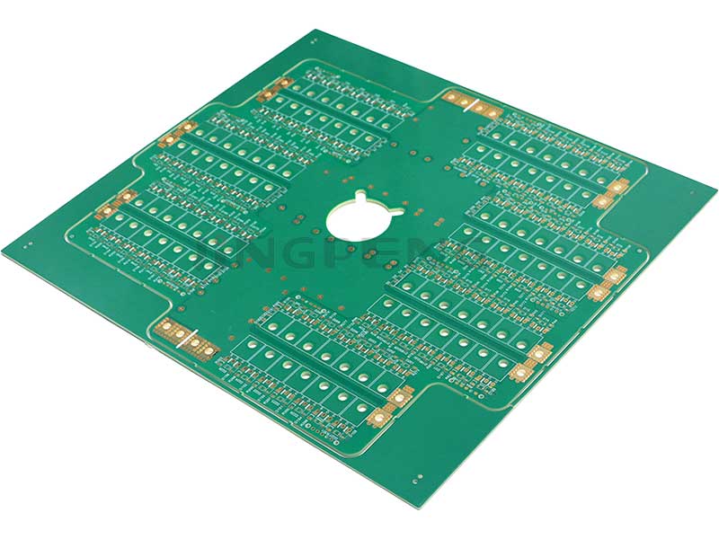
10-layer thick copper board
Focus on multi-layer current paths, copper distribution, and stack-up design.

10-Layer Industrial-Grade Thick-Copper PCB
Pay attention to power, control area layout, and assembly requirements.
The product images illustrate the structural types; specific copper thickness, materials, and applicable environments are subject to the project documentation.
06 / Request for Quotation Materials
Start Your Quote with a Complete Set of Requirements
STEP 01
Manufacturing Documents
Gerber, drill, outline, and layer files; specify the base copper or finished copper thickness, board thickness, material, and surface finish for each layer.
STEP 02
Working Conditions
Continuous/peak current, permissible temperature rise, environmental and thermal conditions, as well as insulation, dielectric strength, and assembly requirements.
STEP 03
Delivery Requirements
Quantity, expected delivery date, and inspection and acceptance requirements; if a PCBA is required, please also provide the BOM and coordinate files.
07 / Frequently Asked Questions
FAQ on Selecting Thick-Copper PCBs
Is a 2-ounce PCB considered a thick copper board?
Terminology may vary among suppliers. On this page, Shenzhen Jingpeng Electronics defines “thick copper PCBs” as those with a copper thickness of 3 oz or more. When requesting a quote, please specify the copper thickness for each layer directly; avoid using only the term “thick copper.”
Does a thicker copper layer necessarily mean a higher allowable current?
Under the same trace width and conditions, increasing the copper thickness helps reduce resistance. However, the design-allowed current is also affected by temperature rise, layer position, adjacent copper surfaces, vias, and heat dissipation conditions; therefore, it cannot be calculated solely based on a fixed current density.
Does increasing the thickness of the copper improve voltage resistance?
You cannot make that determination directly. Dielectric strength must be evaluated in conjunction with the insulating material, dielectric thickness, electrical clearance, creepage distance, and test conditions.
What is the difference between the thickness of the base copper and the thickness of the finished copper?
"Base copper" refers to the initial copper foil thickness; "finished copper thickness" refers to the required thickness after processing, and the outer layer typically involves processes such as electroplating. Manufacturing documents should clearly specify the copper thickness specifications and acceptance criteria.
Do thick-copper PCBs have to use a specific type of copper foil or a high-Tg material?
It is not appropriate to make blanket statements. Materials and copper foil should be selected based on operating temperature, laminate fill, soldering processes, and reliability requirements; material grades and laminate configurations should be confirmed through engineering review.
How do you choose between thick copper plates and metal substrates?
Thick copper boards primarily regulate current-carrying capacity and thermal diffusion by adjusting the thickness of the copper traces; metal substrates emphasize heat transfer from the insulating medium to the metal base layer. The choice should be based on the number of circuit layers, the insulation, and the overall heat dissipation path of the device.
Is it possible to achieve the maximum copper thickness, the highest number of layers, and the smallest via diameter all at the same time?
These conditions cannot be met simultaneously by default. There are restrictions on the combinations of various parameters, which must be evaluated in conjunction with the material, lamination, pore structure, pattern density, and number of patterns.
How are lead times for prototypes and mass production determined?
Material preparation, copper thickness, number of layers, manufacturing processes, and quantity all affect the lead time. After you submit the complete documentation and your desired delivery date, Shenzhen Jingpeng Electronics will confirm a feasible schedule.
Shenzhen Jingpeng Electronics
Turning high-current requirements into feasible solutions
Submit your design files, the copper thickness for each layer, and the operating conditions to receive an engineering evaluation and quote for a thick-copper PCB.
