

This article introduces HDI The five key requirements in production and processing include HDI dimensions, shape design, transmission direction, positioning holes, and optical positioning symbols. Additionally, to improve production efficiency and optimize the manufacturing process, this article discusses optimization strategies and recommendations for each of these requirements. Understanding and adhering to these requirements and strategies will help PCB manufacturers, PCB designers, and PCBA fabricators effectively improve the quality and efficiency of HDI production and fabrication.
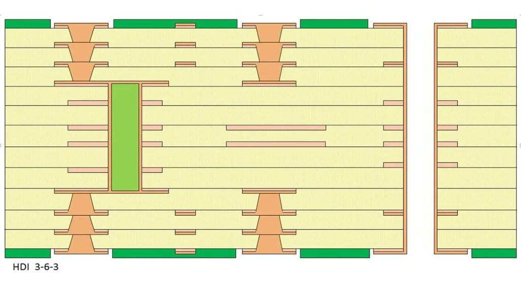
HDI Dimensions
The size of HDI is limited by the production capacity of the equipment on the electronic manufacturing line; therefore, appropriate HDI dimensions should be considered during the design of the product system solution.
- The maximum HDI size that SMT equipment can place is determined by the standard dimensions of HDI sheets, which are typically 20″ × 24″, or 508 mm × 610 mm (guide rail width).
- The recommended dimensions are those for the various pieces of equipment on the SMT production line; they help maximize the production efficiency of each piece of equipment and eliminate bottlenecks.
- Small-size HDIs should be designed as modular assemblies to improve the production efficiency of the entire production line.
Design Requirements:
- Generally, the maximum dimensions of an HDI are limited to 460 mm × 610 mm.
- The recommended size range is (200–250) mm × (250–350) mm, with an aspect ratio of 2.
- HDI boards measuring “125 mm × 125 mm” should be assembled to the appropriate size.
Introduction to HDI
SMT production equipment uses guide rails to transport HDI boards; it cannot transport HDI boards with irregular shapes, especially those with notched corners.
Design Requirements:
- The HDI should be a regular square with rounded corners.
- To ensure stability during the transfer process, irregularly shaped HDI boards must be converted into standard squares by panelizing. In particular, gaps at the edges and corners must be filled to prevent the wave soldering fixtures from getting stuck during transport.
- Notches are permitted on pure SMT boards, but the size of the notch must be less than one-third of the length of the edge on which it is located. If this requirement is exceeded, supplementary measures must be taken in the design and manufacturing processes.
- The chamfer design for the gold fingers requires chamfering at the insertion end; a (1–1.5) × 45° chamfer should also be designed on both sides of the insertion board to facilitate insertion.
Transmission Direction
The dimensions of the drive side depend on the requirements of the equipment’s drive rail. For printing presses, pick-and-place machines, and reflow ovens, the drive side is generally required to be 3.5 mm or wider.
Design Requirements:
- To minimize deformation of the HDI during soldering, the transmission direction is generally set along the long edge of the unassembled HDI; the long edge should also serve as the transmission direction for the layout.
- Typically, two edges of the HDI or board assembly in the direction of signal transmission are designated as signal edges. The minimum width of a signal edge is 5.0 mm. No components or solder joints are permitted on either side of the signal edge.
- There are no restrictions on SMT equipment on the non-transmission side. It is recommended to leave a 2.5 mm no-placement zone around components.
Alignment Holes
Many processes—such as panel assembly, assembly, and testing—require precise positioning of HDI. Therefore, it is generally necessary to design positioning holes.
Design Requirements:
- At least two positioning holes should be designed for each HDI board: one circular and one elongated slot. The former is used for positioning, and the latter for guidance. There are no specific requirements for the diameter of the positioning holes; they may be designed according to factory specifications. Recommended diameters are 2.4 mm and 3.0 mm. Positioning holes should be made of non-metallic material. If the HDI is a perforated HDI, a perforated plate should be designed for the positioning holes to enhance rigidity. The length of the guide hole is generally twice its diameter. The center of the positioning hole should be at least 5.0 mm from the drive side, and the two positioning holes should be as far apart as possible. It is recommended to arrange them diagonally across the HDI.
- For hybrid HDI (HDIA with components installed), the positioning holes must align, and the same fixtures can be used for both the front and back sides. If screws are installed, the bottom bracket can also be used as a component tray.
Locator
Modern surface-mount placement machines, printers, optical inspection equipment (AOI), solder paste inspection equipment (SPI), and other devices all use optical positioning systems. Therefore, optical positioning marks must be designed on HDI boards.
Design Requirements:
- Alignment marks are classified as global fiducials and local fiducials. The former are used for aligning the entire board, while the latter are used for aligning assembled sub-boards or fine-pitch components.
- Optical alignment marks may be designed as squares, diamonds, circles, crosses, or grid patterns, with a height of 2.0 mm. It is generally recommended to design a circular copper alignment mark with a diameter of 1.0 m. To ensure sufficient contrast between the material color and the surrounding environment, an unobstructed soldering area 1 mm larger than the optical alignment symbol should be reserved. No characters are permitted within this area. The presence of copper foil within the inner layers of the three symbols on the same board must be consistent.
- On the HDI side of the surface-mount component board, it is recommended to place three full-board optical alignment marks at the corners of the board to facilitate 3D alignment of the HDI (three points define a plane, which can be used to measure the board’s thickness) and solder paste.
- During assembly, in addition to the three optical alignment marks on the entire board, it is recommended to design two or three assembly optical alignment marks at the corners of each sub-board.
- For devices such as QFPs with a lead pitch of ≤0.5 mm and BGAs with a lead pitch of ≤0.8 mm, local optical alignment marks should be placed diagonally to facilitate accurate positioning.
- If components are mounted on both sides, each side should have optical alignment marks.
- If there are no registration holes on the HDI board, the center of the optical registration mark must be at least 6.5 mm away from the HDI transmission side. If there are registration holes on the HDI board, the center of the optical registration mark should be positioned on the side of the registration holes closest to the center of the HDI board. PCB manufacturers, PCB designers, and PCBA manufacturers will explain the five requirements for HDI production and processing.
