

Concepts of PCB Thickness and Copper Thickness
During the cutting process for PCB fabrication, board thickness and copper thickness are important factors to consider. Generally, for board thicknesses greater than 0.8 millimeters, the standard series includes 1.0, 1.2, 1.6, 2.0, and 3.2 millimeters. For non-standard series with board thicknesses less than 0.8 millimeters, commonly used thicknesses include 0.1, 0.15, 0.2, 0.3, 0.4, and 0.6 millimeters.
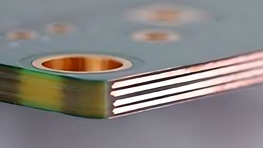
The Impact of Board Thickness on PCB Design
When designing the outer layer of a PCB, several factors must be considered when selecting the board thickness. The manufacturing process requires accounting for the thickness of the copper plating, solder mask, surface treatments (such as tin plating and gold plating), as well as the thickness of characters and carbon ink. In actual production, finished metal-clad laminates tend to be 0.05–0.1 millimeters thicker than specified, while tin-clad laminates tend to be 0.075–0.15 millimeters thicker. Therefore, selecting an appropriate board thickness during the design phase to meet the requirements of the final product is crucial.
The Importance of Copper Thickness in Design
Copper thickness is also one of the key factors affecting PCB design. Different circuits require different copper thicknesses, and the choice of copper thickness affects the PCB’s electrical performance, heat dissipation, and soldering quality, among other aspects. Selecting the appropriate copper thickness based on circuit requirements ensures the stability and performance of the PCB.
Tolerances for Board Thickness and Copper Thickness
During the PCB design process, it is necessary to consider not only product assembly tolerances but also factors such as incoming board material tolerances, lamination tolerances, and outer layer thickness tolerances. These tolerances affect the final board thickness of the finished product. Typical board material tolerances are ±0.1 millimeters for thicknesses between 0.8 and 1.0 millimeters, ±0.13 millimeters for thicknesses between 1.2 and 1.6 millimeters, ±0.18 millimeters for 2.0 millimeters, and ±0.23 millimeters for 3.0 millimeters. Lamination tolerances depend on the number of layers and the panel thickness, and are generally controlled within a range of ±0.05–0.1 millimeters.
The Relationship Between Surface Copper Thickness and Electrolytic Copper Deposition
The issue of surface copper thickness must also be considered during the PCB manufacturing process. Via copper is applied through chemical copper plating and electroplating; increasing the via copper thickness will affect the surface copper thickness. According to the IPC-A-600G standard, the minimum copper plating thickness is 20 µm (Class 1 and 2) and 25 µm (Class 3). Therefore, during production, if a copper thickness of 1 oz (minimum 30.9 µm) is required, the board material may be cut from 0.5 oz (minimum 15.4 µm) sheet. The choice of board material affects the final copper thickness.
Board thickness and copper thickness are key factors that must be carefully considered during the PCB design process, as they directly affect the performance and stability of the final product. Proper design and adjustments can ensure the success and quality of PCB manufacturing.
Frequently Asked Questions (FAQs)
1. How do board thickness and copper thickness affect PCB performance?
The thickness of the board and the copper layer affect the circuit board’s electrical performance, heat dissipation, and soldering quality, among other factors, and directly impact the performance of the final product.
2. How can the board thickness and copper thickness be adjusted to meet design requirements?
Based on the design requirements, you can select an appropriate board thickness when designing the outer-layer PCB; the desired thickness can be achieved by choosing the right board material and adjusting the laminate structure.
3. What are the tolerances for board thickness and copper thickness in PCB design?
For standard sheet materials with a thickness range of 0.8–3.0 millimeters, the thickness tolerance is between ±0.1 and 0.23 millimeters, and the lamination tolerance is between ±0.05 and 0.1 millimeters.
4. Why is the thickness of the copper coating related to electroless copper plating?
The surface copper thickness must be achieved through chemical copper plating and electroplating. Thickening the copper in the holes affects the surface copper thickness, so the relationship between the two must be taken into account.
5. How can we ensure the stability and performance of a PCB?
By carefully selecting the board thickness and copper thickness, taking tolerances into account, and designing and adjusting the PCB according to circuit requirements, you can ensure its stability and performance.
