



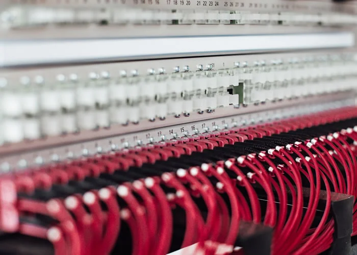



Advantages and Disadvantages of Prototype Board Design in PCB Design
2026-10-20
Read the article ↗From PCB prototyping and professional board manufacturing to component procurement, SMT assembly, and testing, each delivery milestone is linked by a clear engineering review process.
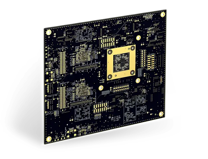
From connection density to full-board implementation
HDI · IC Substrates · Rigid-Flex · High-Frequency · PCBA
First, verify the materials, laminate structure, and manufacturing constraints.
PCB and PCBA Services by Project Portfolio
Clarify inspection items, documentation, and acceptance criteria
PRODUCTS / PCB
Based on interconnect structure, frequency, thermal management, and packaging requirements, we will select a product direction and then jointly confirm a manufacturable solution.
Evaluate microvias, blind and buried vias, and multilayer structures for high-density wiring and fine-pitch components.
Learn More ↗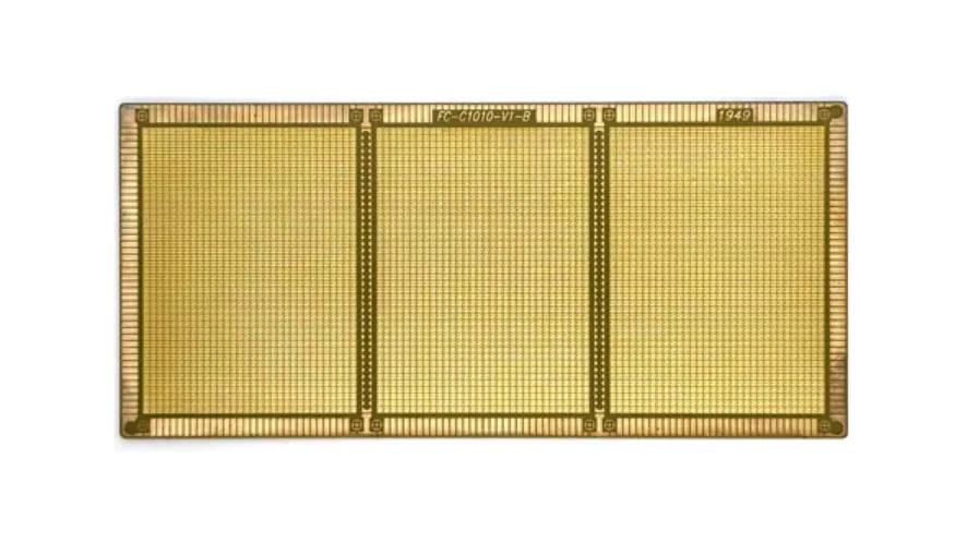
Conduct a process feasibility review focusing on packaging formats, interconnect density, and warpage requirements.
Learn More ↗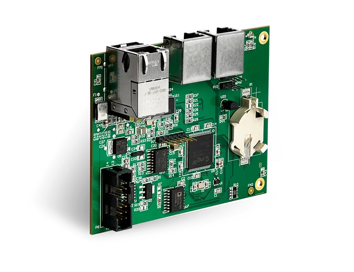
Integrates the requirements of PCB manufacturing, material preparation, SMT assembly, and testing.
Learn More ↗SERVICES / FROM FILES TO ASSEMBLY
You may choose individual services or a combination of services based on your project needs; please clarify the scope of services, the method of material supply, and testing responsibilities before we provide a quote.
01
Review risks related to manufacturing and assembly, and compile a list of issues that need to be addressed.
View Services ↗02
Finalize the manufacturing plan based on the materials, stacking, vias, and surface treatment.
View Services ↗03
Organize collaboration based on the approved BOM, substitution rules, and assembly requirements.
View Services ↗04
Determine the scope of application for AOI, X-ray, electrical testing, or functional testing on a project-by-project basis.
View Services ↗
Shenzhen Jingpeng Electronics coordinates efforts around engineering documentation, production processes, and inspection records to ensure that product requirements are clearly verified before delivery.
Materials, board thickness, layer count, impedance, and special requirements form a consistent set of engineering inputs.
Select inspection items based on product structure and order requirements, focusing on critical processes and traceability data.
Testing, packaging, labeling, and shipping documents will be mutually confirmed at the start of the project.
APPLICATIONS / ENGINEERING CONTEXT
Organize the signal, thermal, mechanical, and reliability requirements by application environment, then visit the corresponding industry page to learn about the key points for project evaluation.

Temperature Cycling, Assembly, and Traceability Requirements
Learn About the App ↗WORKFLOW / START A PROJECT
Whether it’s your first prototype or an iterative update, start by clearly defining the key inputs so that reviews and quotes have a solid foundation.
PCB files, quantities, and board specifications; for PCBA projects, please also provide a BOM, coordinates, and test requirements.
Jointly review the stacking, manufacturing constraints, materials, and acceptance requirements, and identify issues that need to be resolved.
Specify the technical solution, costs, scheduled delivery date, and the scope of delivery agreed upon by both parties.
Conduct production and inspection in accordance with the approved documentation, and complete packaging and document delivery as agreed.
RESOURCES / DESIGN WITH CONFIDENCE
Make preliminary selections regarding materials and processes to minimize information gaps and the need for repeated confirmations.
Learn about the key considerations for selecting FR-4, PTFE, polyimide, and materials from leading brands.
Reading Guide ↗Compare the process paths and design constraints of through-holes, blind and buried vias, microvias, and in-pad vias.
Reading Guide ↗Select a surface treatment method based on welding, contact, storage, and assembly requirements.
Reading Guide ↗INSIGHTS / BLOG
Read articles on PCB design, materials, and manufacturing to ensure your project is technically well-prepared from the design phase onward.
2026-10-20
Read the article ↗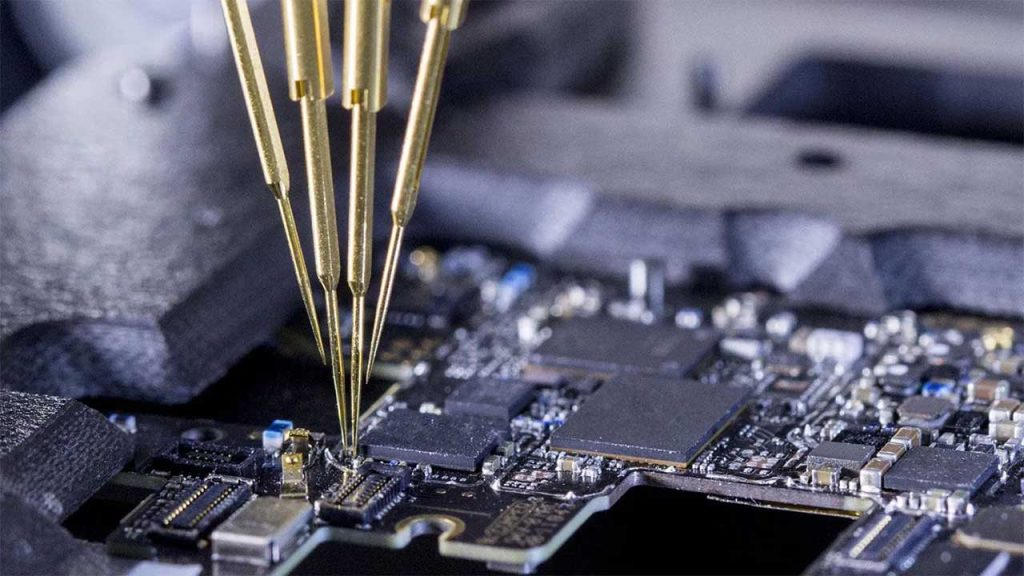
2026-10-20
Read the article ↗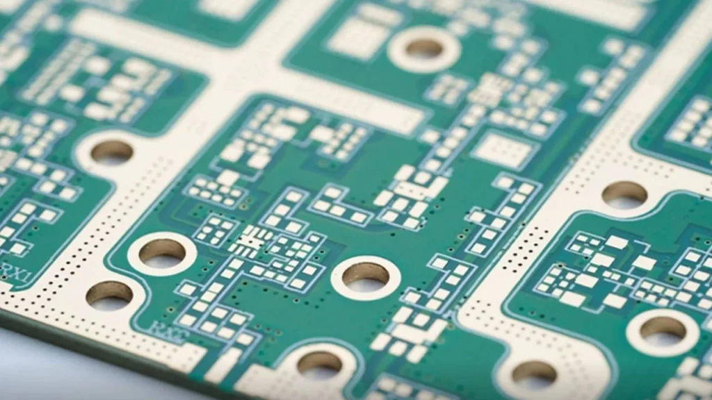
2026-10-20
Read the article ↗2026-10-20
Read the article ↗2026-10-19
Read the article ↗2026-10-19
Read the article ↗LET’S BUILD YOUR NEXT PCB
Please send us your Gerber files, BOM, or project requirements so we can first confirm the technical approach before proceeding with a quote and delivery schedule.
Don't have all the details yet? You can start by describing the application, board type, quantity, and current stage.
