

Radar PCBs From RF Design to Stable Manufacturing
Clearly define manufacturing requirements in advance for the materials, laminates, RF traces, and antenna areas of your radar project. Shenzhen Jingpeng Electronics will conduct a manufacturability review based on your design documents, ensuring that both prototyping and subsequent production are carried out in accordance with established guidelines.
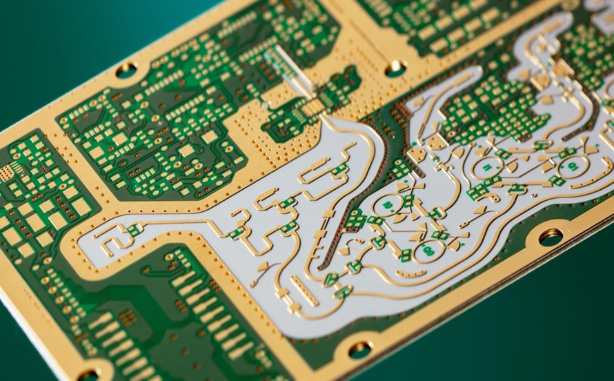
Radar PCB Product Showcase | Specific materials and processes are subject to confirmation in project documentation
Materials and Layers
Verify the model, material, and copper thickness
Radio Frequency and Antennas
Define Geometry, Window Areas, and No-Plot Zones
Documents and Inspections
Standardized Version and Acceptance Requirements
01 / Define the Architecture
First, determine where the antenna is located, then decide on the PCB design.
Radar PCBs carry electrical interconnects and may incorporate antennas. Detection range, angular accuracy, and target identification also depend on the chip, antenna, algorithms, installation environment, and system calibration.
PCB-Integrated Antenna
Antenna patterns are directly fabricated on the PCB. The review should focus on dielectric thickness, material parameters, copper surface roughness, pattern dimensions, as well as the solder mask and surrounding structures in the antenna area.
Antenna-on-Package (AoP)
The antenna is integrated into the chip package; the motherboard design must comply with the chip reference design. Just because a project involves millimeter-wave radar does not mean the entire board must use the same type of high-frequency material.
External Antenna or RF Module
Pay particular attention to connector or module interfaces, feedline impedance, reference ground, power supply, and mechanical connections. Manufacturing documentation should clearly define the boundaries between the main board, RF subboard, and modules.
02 / Materials and Layering
Ensure that the material selection matches the actual RF path
Loss and Uniformity in the RF Layer
Compare the dielectric constant, loss factor, and test conditions corresponding to the operating frequency bands, while also considering the type of copper foil, surface roughness, and dielectric thickness. Parameters obtained using different test methods should not be directly compared on an equivalent basis.
High-Frequency Materials and Hybrid Pressing Solutions
Evaluate high-frequency materials or mixed-pressure laminates based on the chip reference design and electrical requirements. For mixed-pressure laminates, it is necessary to verify the material combination, press compatibility, interlayer structure, and thermal reliability.
Digital, Power, and Cooling Zones
Arrange the stack-up to accommodate digital interfaces, power supply, grounding, and device thermal management requirements. Any substitution of materials or structural adjustments must be approved by the design team to avoid replacing materials solely based on price.
03 / Manufacturing Review
Include key requirements in production documentation
Quotes for radar projects should not be based solely on the number of layers and board thickness. The following items should be confirmed along with the documentation; achievable tolerances and inspection plans are subject to the results of the engineering review.
- Material Model
- Complete part numbers, copper foil types, dielectric thickness, and whether substitute materials are permitted.
- Layer Stacking and Copper Thickness
- Uses of each layer, reference planes, and requirements for finished board thickness and copper thickness; mixed-press structures must be confirmed separately.
- RF Tracing
- Impedance targets, tolerances, trace widths and spacing, reference grounds, and RF networks requiring special attention.
- Vias and Layer Transitions
- Requirements for aperture size, pads, back-drilled holes, or blind/buried vias, as well as stump requirements; to be reviewed based on the actual structure.
- Antennas and Surface Treatment
- Antenna geometry, no-solder zones, solder mask openings, and surface treatment areas—avoid applying the same default rules to the entire board.
- Inspection and Delivery
- Electrical testing, impedance testing, and reporting requirements; high-frequency test procedures and acceptance criteria are to be agreed upon separately.
04 / Applications and Validation
Identify key verification areas based on usage scenarios
Automotive and Transportation Sensing
Consider the effects of temperature fluctuations, vibration, power supply noise, and mounting structures on the system. For in-vehicle applications, the applicable quality and reliability requirements must be verified separately.
Industrial Distance Measurement and Level Measurement
Consider ambient temperature, the medium and housing, the antenna field of view, and long-term stability. PCB structure and assembly constraints must be jointly verified during the design phase.
Presence Sensing and Smart Devices
Evaluate solutions based on space, power consumption, digital interfaces, and enclosure design. Detection coverage and false alarm performance must be verified in real-world operating environments.
There are three types of verification: bare board electrical testing to check for open circuits and short circuits; PCBA testing to verify assembly and circuit functionality; and radar system testing to verify RF and detection performance. A passing bare board test does not mean that the system’s performance has been verified.
05 / Request for Quotation Materials
Provide clear information the first time to reduce the need for repeated confirmation
01 · Production Data
Gerber or ODB++ files, drill files, board dimensions, and mechanical drawings. Please specify the file version and ensure that all files correspond to the same design.
02 · Process and RF Requirements
Material grade, stack-up, board thickness, copper thickness, impedance specifications, surface treatment, and any special requirements for the antenna area; if you have a reference stack-up, please provide it as well.
03 · Quantity and Delivery Requirements
Prototyping and subsequent order quantities, desired delivery dates, inspection items, and reporting requirements. If assembly or final product validation is involved, please specify the scope of services.
06 / Frequently Asked Questions
Frequently Asked Questions About Radar PCB Projects
Do radar PCBs have to use high-frequency materials?
Not necessarily. First, distinguish between different architectures—such as PCB antennas, package antennas, and external modules—and then select materials based on the RF path, chip reference design, and loss requirements. The specific materials and stack-up are confirmed by both the design and manufacturing teams.
Can standard FR-4 be used as a substitute for the specified RF material?
They should not be substituted directly. Changes in the dielectric constant, loss, thickness, and copper layer characteristics may affect impedance and antenna performance. Alternative solutions should be reevaluated and verified by the design team.
Does passing the impedance test guarantee radar performance?
No. Impedance testing is specific to defined structures and test methods; radar performance also involves high-frequency losses, antennas, the RF front end, assembly, the enclosure, and algorithms, and requires verification at the system level.
Can we manufacture directly based on the chip reference board?
You will need complete and authorized production data, and you must verify the reference design version, materials, stack-up, and manufacturing notes. If you modify the board layout, antennas, or materials, you cannot assume that performance will be the same as that of the reference board.
What documents are required for a radar PCB quote?
Please provide Gerber or ODB++ files, drilling specifications, stack-up, material, and process requirements, and specify the quantity, delivery date, and testing requirements. Critical dimensions for RF or antenna components should be clearly marked on the drawings.
Does this include assembly and radar system testing?
Bare board, component mounting, and finished product testing fall under different scope of work. When submitting a request for quotation, please list the required services, component specifications, test methods, and acceptance criteria; the work will proceed once these details have been clarified by both parties.
How do you determine achievable machining tolerances and delivery times?
The final decision will be based on a review of the complete documentation. Material availability, lamination, via patterns, critical geometries, and inspection items will all affect manufacturability and scheduling; quotes and delivery arrangements will be finalized after these requirements are confirmed.
Technical Reference:TI Packaged Antenna Radar Reference Design · TI Millimeter-Wave Radar Installation and Angulation Guide. The reference materials are provided to illustrate design considerations and do not represent the Company’s manufacturing capabilities or product certifications.
Shenzhen Jingpeng Electronics
Submit Your Radar PCB Requirements for Engineering Review
From materials and laminates to key RF areas, first confirm the manufacturing constraints, then proceed with the quote and prototyping.
