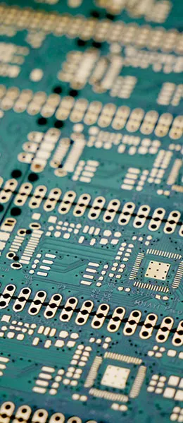
PCB design is a critical step in the manufacturing of electronic products. It not only serves as the physical foundation for electronic products but also directly impacts their performance, stability, reliability, and the ease of production and maintenance. In this article, we will take an in-depth look at the key elements of PCB design, as well as the knowledge framework that an outstanding PCB engineer should possess.
Advanced: What Are the Strengths of Each Major EDA Tool?
| Tools | Areas of Strength | Typical Users | Cost of Learning |
|---|---|---|---|
| Cadence Allegro | Rule-driven, large-scale projects, high-speed constraints | Communications, Servers, Industrial Control | 高 |
| Mentor Xpedition | Team Collaboration, Enterprise-Level Processes | Large R&D Organization | 高 |
| Mentor PADS | Easy to get started with and great value for the price | Small and Medium-Sized Enterprises, Consumer Goods | 中 |
| Altium Designer | Consistent user interface, comprehensive libraries and ecosystem | Startup teams, individual developers | Low to medium |
| Open-source tools such as KiCad | Zero Cost, Active Community | Learning, Open-Source Hardware | 低 |
The key to choosing a tool isn't the number of features it has, but ratherCan Constraint Management Support the Complexity of a Project?. The more complex the board and the more rules there are, the greater the value of constraint-driven design. Using heavy-duty tools on simple boards actually slows things down.
- Looking at the Team and Supply Chain: Use whatever your collaborators use as much as possible to minimize the cost of file exchange;
- View Device Libraries and Package Resources: The quality of the library directly determines design efficiency and the error rate;
- Consider Constraint Capability: The degree of automation in differential pair, equal-length, and impedance rules has a significant impact on high-speed boards.

See the prototyping iteration speedSpeed of PCB Design Prototype Iteration; For the proofing process, seeA Detailed Explanation of the PCB Prototyping Process and Key Considerations。
1. Familiarity with mainstream EDA tools
There is a wide variety of PCB design software available, with the most commonly used options on the market including Cadence Allegro, Mentor EE, Mentor Pads, and Altium Designer. Among these, Cadence Allegro has the highest market share and is highly popular due to its user-friendly interface, fast response times, high operational efficiency, and comprehensive rule manager features. Allegro also performs exceptionally well on large-scale projects, maintaining high responsiveness. As a result, Allegro is an ideal choice for sectors such as telecommunications, commercial servers, industrial control, and defense.
2. Familiarity with components and circuit schematics
A basic understanding of common electronic components—such as resistors, capacitors, inductors, diodes, and transistors—as well as the ability to read circuit schematics, are essential skills for PCB design engineers. This helps them understand the functionality and performance requirements of circuits.
Advanced: Four Parameters for Selecting Panels
"Understanding circuit board materials" isn't just about memorizing FR-4 and aluminum substrates; it's about being able to interpret four key parameters and make trade-offs based on project requirements:
| Parameters | Meaning | Impact |
|---|---|---|
| Tg (glass transition temperature) | The temperature at which the material begins to soften | Reflow Endurance and High-Temperature Stability |
| Td (Decomposition Temperature) | The temperature at which a material undergoes chemical decomposition | Upper Heat Resistance Limit and Processing Window |
| Dk (Dielectric Constant) | Factors Affecting Impedance and Signal Speed | Impedance Calculations and Trace Width |
| Df (tangent of the loss angle) | Magnitude of Dielectric Loss | High-Frequency Insertion Loss and Signal Integrity |
- Lead-free processes require a higher Tg: Lead-free reflow temperatures are higher, and materials with low Tg are prone to delamination;
- For high-frequency scenarios, start by looking at Df: The tangent of the loss angle has a more direct effect on insertion loss than the dielectric constant;
- Td: Determining the Machining Allowance: The narrower the window between Td and the processing temperature, the more difficult it is to control the process.

For information on how to select sheet materials, seeHow to Choose the Right PCB Material Based on PCB Type; For the material system, seePCB Materials。
3. Familiarity with different types of sheet materials and manufacturing processes
Different electronic products require different types of board materials and manufacturing processes. Familiarity with commonly used board materials—such as FR-4 fiberglass boards and aluminum-based boards—as well as an understanding of the manufacturing processes and technical requirements of various PCB manufacturers, will help you select the appropriate materials and manufacturing partners.
4. Familiarity with surface-mount and through-hole assembly
Understanding assembly processes such as surface-mount technology (SMT) and through-hole technology (THT) can help optimize circuit board design and improve production efficiency and reliability.
5. Understanding Welding Testing
Soldering quality directly affects the quality of the entire device, so solderability testing is crucial. It is used to evaluate the solderability of components, circuit boards, solder, and flux. Scientific solderability testing helps improve soldering quality.
Advanced: Practical Checklist for SI and PI
Signal integrity and power integrity may sound abstract, but when it comes to design verification, they actually involve the following specific steps:
- Check Reference Plane Continuity: Is there a complete plane beneath the high-speed signal, and does it cross the median?;
- Check the return path: Are there via holes at the layer change points, and can the reflow process follow them?
- Check Termination: Are resistors installed on the network that needs to be terminated, and are they in the correct positions?;
- Check for equal length: Is the difference in length between the bus and the differential pair within the allowable range?;
- Check the layout of the decoupling capacitors: Is the capacitor located close to the power supply pin, and is the return path short?;
- Check the Planar Impedance: Is the spacing between the power and ground planes small enough to reduce the plane impedance?
Question 5 is the one most likely to be answered incorrectly.The capacitance value of decoupling capacitors is important, but their placement is even more important.: If a capacitor is placed too far away, the inductance of its leads will negate most of the high-frequency decoupling effect. The determining factor is whether the return path from the capacitor to the power supply pin is sufficiently short.
- Multiple Capacitors in Parallel: Cover different frequency bands; be mindful of anti-resonance issues;
- Place vias as close to the pads as possible: Shorten the path to the plane;
- Simulate Critical Networks First: Simulation is used to compare the merits of different approaches, not to replace actual testing.

For an overview of signal integrity, seeSignal Integrity Issues in PCB Design; For the electrostatic protection design, seeElectrostatic Protection Design for PCBs。
6. Master SI/PI Concepts
Signal integrity (SI) and power integrity (PI) are critical considerations in high-speed digital PCB design. SI takes into account factors such as circuit parameters, component placement, and signal routing, while PI focuses on power path design and decoupling capacitor design. This knowledge helps optimize PCB design and improve performance and reliability.
7. In-Depth Understanding of EMC/EMI
Electromagnetic Compatibility (EMC) and electromagnetic interference (EMI) are issues that must be considered in the design of electronic products. EMI issues can cause system instability, so PCB design plays a critical role in addressing EMI. A thorough understanding of these issues is essential for designing high-performance electronic products.
Advanced: Six Self-Checks Before Production
- Package Verification: Carefully compare the device package with the actual datasheet, paying particular attention to pin spacing;
- Online-to-Paper Reconciliation: The schematic matches the PCB netlist; there are no floating networks or short circuits;
- Rule Verification: Are the design rules set according to the PCB manufacturer's capabilities rather than the software's default values?;
- Document Verification: Complete Gerber layers, matching drill files, and no missing inner layers;
- Process Verification: Are the surface treatment, solder mask color, board thickness, and impedance requirements clearly specified?;
- Assembly Check: Check whether the components interfere with each other, whether the silkscreen overlaps the solder pads, and whether the alignment holes are properly positioned.
These six items represent the most cost-effective quality assurance measures during the prototyping phase. Although the prototyping cycle is short and the unit price may seem low,A failed prototype wastes project time....are often much more valuable than the cost of the board itself.
- Test points should be included on the first board.: Leave test points on critical circuits to facilitate debugging and jumper wiring;
- Key parameters remain adjustable: Set the power supply feedback resistor, termination resistor, and other resistors to 0 Ω or an adjustable position;
- List of Issues to Be Documented: Make a note of any issues that arise during each proof run, and address them one by one in the next version.

See "Responding to Component Shortages"How Component Shortages Affect Electronic Product Design and How to Avoid Them; For manufacturing capabilities, seePCB Manufacturing Capabilities。
In the field of PCB design, mastering this knowledge and these skills will make you an outstanding engineer. PCB design is not merely a technical discipline—it is also an art. Through continuous learning and practice, you will be able to design exceptional PCBs that meet requirements such as high cost-effectiveness, excellent electrical performance, stability and reliability, ease of manufacturing and repair, and ease of certification.
Conclusion
PCB design is a core component of electronic product manufacturing and determines a product’s performance and quality. An outstanding PCB engineer must possess a broad range of knowledge and skills to meet ever-changing market demands. A deep understanding of EDA tools, components, PCB materials, manufacturing processes, soldering, SI/PI, and EMC/EMI will help you succeed in the field of PCB design.
Advanced: The Minimum Action Required in EMC Design
EMC is a broad topic, but for most projects, implementing the following cost-effective measures will cover the majority of risks:
- Ensure the surface is intact: This is the foundation of all EMC measures; if the ground plane is incomplete, subsequent measures will have limited effectiveness;
- Set aside the interface filtering: ESD and filtering components are mounted directly adjacent to the connector to block interference from entering the board;
- Clock is handled separately: Shortest path, enclose the area, do not draw lines below;
- Consider Cables and Shielding Together: External cables are often the primary source of radiation; don't just focus on the board itself;
- Allow room for corrective action: Reserve filtering and shielding pads at key locations to allow for future modifications.
The last one is a common practice among senior engineers:Set aside space for possible modifications during the initial design phase. These reserved pads do not need to be populated after the test is passed; the cost is virtually zero, yet they can save a round of PCB rework during rectification.

For noise-reduction tips, see16 Tips for Reducing Noise and Electromagnetic Interference in Printed Circuit Boards; for layered stacking and EMI, seeThe Role of PCB Layer Stacking Design in Suppressing EMI。
Frequently Asked Questions
1. What is PCB design?
PCB design refers to the design of printed circuit boards, which serve as the substrate in electronic products for supporting and connecting electronic components. PCB design determines the performance and reliability of electronic products.
2. Why is PCB design so important?
PCB design directly affects the performance, stability, and reliability of electronic products. A well-designed PCB can improve a product’s cost-effectiveness and reduce production and repair costs.
3. What are some of the most popular PCB design software programs?
Popular PCB design software includes Cadence Allegro, Mentor EE, Mentor Pads, Altium Designer, and others. Choosing the right software depends on project requirements and personal preference.
4. What are EMC and EMI?
EMC stands for electromagnetic compatibility and refers to the ability of electronic products to operate in an electromagnetic environment without causing or being subject to interference. EMI stands for electromagnetic interference and refers to the interference caused to other devices by electromagnetic waves emitted by electronic equipment. These two factors are critical in the design of electronic products and require in-depth understanding and proper handling.
5. How can you improve the performance of a PCB design?
To improve the performance of PCB designs, it is necessary to select appropriate components, optimize circuit layout, ensure signal integrity and power integrity, and address issues such as electromagnetic compatibility and electromagnetic interference. Continuous learning and hands-on practice are also key to improving design skills.
6. What area of knowledge should a new engineer focus on first?
I suggest you start by brushing up on manufacturing processes. For most new designers, the problem isn’t a lack of understanding of circuit theory, but rather a lack of awareness of what PCB manufacturers can and cannot do. Once you understand the limitations of drilling, etching, and lamination, the quality of your designs will immediately improve—and this is the area where you’ll see results the fastest.
7. What should you do if there is a mismatch between design rules and the PCB manufacturer’s capabilities?
This depends on the board manufacturer’s capabilities. The procedure involves requesting a capability table from the board manufacturer and directly importing parameters such as minimum trace width and spacing, minimum hole diameter, solder ring requirements, and maximum thickness-to-diameter ratio into the EDA design rules. Issues with boards designed using default values are often not discovered until the boards are sent for production.
8. Is simulation absolutely necessary for high-speed boards?
It depends on the data rate and the project’s risk level. For designs operating at several Gbps or with many critical links, simulation can significantly reduce the risk of board redesign; for scenarios with data rates below several hundred Mbps and simple routing, design rules and experience are usually sufficient. A middle-ground approach is to perform simulation only on the one or two most critical links.
9. Will there be any issues if the same set of files is used for both proofing and mass production?
Generally, this is possible, but there are two points to keep in mind: First, the process parameters approved during prototyping may need to be fine-tuned during mass production to ensure a stable yield rate; second, the panel layout should be redesigned during the mass production phase to improve utilization. Therefore, a process validation session should be conducted with the PCB manufacturer before mass production begins.
10. How can I quickly develop the ability to evaluate sheet materials?
The most effective approach is to study failure case studies and wafer inspection reports. Correlating Dk, Df, Tg, and Td with actual problems provides a deeper understanding than simply reviewing parameter tables. In addition, frequent communication with process engineers at wafer fabs can yield insights not found in parameter tables.
11. What should I do first if I fail the EMC test?
First, locate the source of interference corresponding to the frequency points that exceed the limits, rather than immediately applying shielding or filtering. To do this, trace back from the frequency points to identify potential radiation sources on the board (such as clocks, switching power supplies, and data buses), and use the process of elimination to verify by turning them off or reducing their speed one by one. Once the source is accurately identified, the corrective measures are usually quite simple.
Additional Information:A Detailed Explanation of the PCB Prototyping Process and Key Considerations · How Component Shortages Affect Electronic Product Design and How to Avoid Them