Constraints on Trace Routing for Fine-Pitch BGAs
When through-hole solutions cannot provide effective routing in the BGA area, consider laser-drilled blind vias, via-in-pad, and HDI stack-ups.
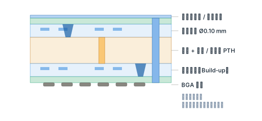
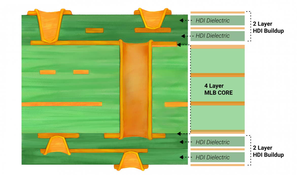
Mass production capabilities are standardized for first-order (1+N+1) and second-order (2+N+2) HDI; third-order (3+N+3) and any-layer interconnect (ELIC) are subject to case-by-case evaluation based on stack-up, microvia structure, and alignment requirements. Minimum line width/spacing for mass production is 0.075 mm, and laser blind via diameter is 0.10 mm. We support the design of blind vias, buried vias, offset vias, stacked vias, and in-pad vias, offering one-stop delivery from prototype validation to mass production.
Laser Blind Vias + Buried Vias / Plated Through-Holes Hybrid Interconnects
The value of HDI lies in using laser microvias and sequential layering to free up routing space, rather than simply pursuing higher-order structures. Starting with an assessment of component, routing, and reliability constraints is typically more effective than directly specifying “first-order, second-order, or third-order” structures.
When through-hole solutions cannot provide effective routing in the BGA area, consider laser-drilled blind vias, via-in-pad, and HDI stack-ups.
The microporous structure directly affects the number of compression cycles, the pore-filling process, yield, and cost. When space permits, one should not overuse stacked pores simply to achieve a “higher order.”
High-speed projects require a simultaneous evaluation of material Dk/Df, dielectric thickness, line width, copper thickness, back drilling, and via stubs—not just the number of HDI layers.
Extreme prototype parameters do not equate to a stable mass production window. During the NPI phase, materials, stack-ups, microporous structures, inspection methods, and acceptance criteria should be finalized in advance.
The number of layers directly determines routing density, manufacturing complexity, and cost. The BGA pitch can serve as a preliminary reference, but it cannot alone determine the number of HDI layers. The table below is intended for quick screening; the final design must undergo a DFM review that takes into account BGA routing, stack-up, microvia structure, impedance, board thickness, and reliability requirements.
| Order | Structural Representation | Applicable BGA Pitch | Laser Aperture | Interlayer Alignment Accuracy * | Mass Production Status |
|---|---|---|---|---|---|
| First-Order HDI | 1+N+1 | 0.5 mm | 0.10 mm | ± 25 μm | Mass Production Standards |
| Second-Order HDI | 2+N+2 | 0.4 mm | 0.075 to 0.10 mm | ± 20 μm | Mass Production Standards |
| Third-Order HDI | 3+N+3 | 0.3 mm | 0.075 mm | ± 15 μm | Prototyping Limits · Mass Production Requires Review |
| HDI on Any Layer | ELIC / Any-layer | < 0.3 mm | 0.075 mm (thinner diameters require evaluation) | ± 10 μm | Special Assessment |
The current mass production standard for laser drilling is 0.10 mm, with a prototyping limit of 0.075 mm. Third-order structures and any-layer (ELIC) designs require higher interlayer alignment accuracy. Quotes will be provided only after a specialized evaluation that takes into account the specific stack-up, number of lamination passes, and alignment capabilities; we do not make direct commitments based on standard capabilities. Interlayer alignment accuracy is provided for reference only; please have it verified by engineering.
Swipe left or right to view the full specifications
0.5 mm
BGA pitch
↓First-Order HDI
1+N+1
0.4 mm
BGA pitch
↓Second-Order HDI
2+N+2
0.3 mm
BGA pitch
↓Third-Order HDI
3+N+3
< 0.3 mm
BGA pitch
↓ELIC on Any Layer
A special assessment is required
When space permits, prioritize offset holes, as this can significantly reduce machining risks and costs.
| Comparison Items | Stacked Via | Staggered Via |
|---|---|---|
| Structural Features | The blind holes on the upper layer and the blind holes on the lower layer are stacked vertically at the same location. | The blind holes on the upper layer are offset from those on the lower layer and are not stacked vertically. |
| Wiring Density | Taller, takes up less space | Lower, but takes up relatively more space |
| Difficulty of Processing | High: Requires through-hole plating + precise alignment | Lower; no need for hole-filling electroplating |
| Reliability Requirements | Specify the IPC-4761 Type VII hole-filling specifications. | Standard processes are sufficient |
| Cost Impact | Add 2 to 3 additional pressing and hole-filling steps | Fewer production steps, shorter lead times |
| Jingpeng PCB Capabilities | Supports second-order and higher-order stacked via designs (subject to review) | Supports miscellaneous-hole designs for all order numbers |
The table below breaks down “Standard Mass Production Capabilities” and “Prototyping and Small-Batch Maximum Capabilities.” The standard mass production values represent the capabilities that can be specified in a contract; the maximum values must be confirmed following a review of the specific stack-up and layout.
| Parameter Items | Mass Production Capabilities | Prototyping · Pushing the Limits | Notes and Explanations |
|---|---|---|---|
| Range of Floors | Floors 4–16 | Floors 4–32 | Includes HDI laminates and multilayer boards |
| HDI Order | 1+N+1 / 2+N+2 | 3+N+3 | Any Layer (ELIC) requires a special review |
| Minimum Line Width / Spacing | 0.075 / 0.075 mm | 0.05 / 0.05 mm | Fine-line circuits rely on the LDI exposure process |
| Minimum Laser Drilling Hole Diameter | 0.10 mm | 0.075 mm | Laser hole aspect ratio ≤ 1:1 |
| Minimum Mechanical Drilling Diameter | 0.20 mm | 0.15 mm | Aspect ratio of machined holes: ≤ 12:1 |
| Thickness of the finished panel | 0.8 to 3.2 mm | 0.4 to 3.2 mm | For ultra-thin plates, the symmetry of the laminate must be evaluated. |
| Maximum Panel Size | 457 × 610 mm | 457 × 610 mm | Supports delivery of panelized sheets (stamp holes / V-cuts) |
| Thickness of finished copper | 18–35 μm | 18–70 μm | Hole diameter in accordance with IPC-6012 Class 2: average ≥ 20 μm, single point ≥ 18 μm |
| Impedance Control Tolerances | ± 10% | ± 7% | Single-ended / Differential; TDR test report included with shipment |
| Supporting Substrates | FR4 Standard / Halogen-Free | FR4 High-Performance / Rogers Series | Materials can be selected based on the customer's specified brand and grade |
| Surface Treatment | OSP / ENIG / Tin Plating | Immersion Silver / Electrolytic Gold / Gold Fingers / ENEPIG | Chemical nickel, palladium, and gold can be provided upon request. |
| Standard Delivery Time | 5 to 8 business days | As fast as 72 hours (expedited) | Rush orders are limited to first-order, ≤ 8-layer, standard-stacked designs; production scheduling confirmation is required. |
Mass production quotes and lead times are based on “standard mass production capabilities”; prototype limits must be confirmed following an engineering review and do not constitute a default commitment for mass production.
Swipe left or right to view the full specifications
The following are the items most frequently reviewed by the HDI project during the DFM review and mass production ramp-up phases; you can use them to directly compare your design specifications.
| Parameter Items | Capabilities / Specifications | Note |
|---|---|---|
Interlayer Alignment Accuracy * | ± 25 μm (first-order) / ± 15 μm (third-order) | The more times the lamination is repeated, the greater the cumulative alignment tolerance. |
Thickness of the Dielectric Layer in Laser-Drilled Blind Holes * | 0.05 to 0.10 mm | Must match the laser aperture; aspect ratio ≤ 1:1 |
Hole-Filling Methods * | 树脂塞孔 + 电镀盖帽 / 铜填孔 | 对应 IPC-4761 Type VI / Type VII |
盘中孔平整度 VIPPO * | ≤ ± 10 μm | 不平整会导致焊接空洞与立碑 |
最小阻焊桥宽度 * | 0.075 mm(量产)/ 0.05 mm(打样) | 绿色阻焊优于哑光黑等深色阻焊 |
背钻 Back Drill * | 支持,残留短桩 ≤ 0.20 mm | 高速信号改善插损与反射,需指定背钻层与深度 |
| Sheet Thickness Tolerance | ± 10%(≥ 1.0 mm)/ ± 0.10 mm(< 1.0 mm) | 薄板按绝对值管控 |
| 外形公差 | 锣边 ± 0.15 mm / 激光切割 ± 0.05 mm | Laser cutting is recommended for irregular shapes and high-precision contours |
Warpage * | ≤ 0.75%(常规)/ ≤ 0.50%(高精度 SMT) | 不对称叠层为翘曲超标主因 |
| IPC 验收等级 | IPC-6012 Class 2 / Class 3(可指定) | 外观按 IPC-A-600 验收 |
| Reliability Testing | 热冲击 288℃/10s、TCT、HAST、HTS | 按 IPC-TM-650 方法,可出内部报告 |
| 阻抗测试 | TDR 时域反射测试,随货附报告 | 高速项目建议设计阶段提供仿真叠层 |
| Delivery Format | 单板 / 拼板(邮票孔、V-cut) | 真空防静电包装,附干燥剂与批次追溯码 |
带 * 的项目为按典型 HDI 产线规格给出的参考值,正式报价前由工程部门依据您的设计规范逐项核定。
Swipe left or right to view the full specifications
精度需求决定品类,选错品类会直接推高成本。
| Sheets | Minimum Line Width / Spacing | Minimum pore size | Typical Number of Floors | Typical Applications |
|---|---|---|---|---|
| 普通多层板 | 0.15 / 0.15 mm | 0.30 mm(机械) | Floors 4–12 | 工控、电源、通用电子 |
| 一阶 / 二阶 HDI | 0.075 / 0.075 mm | 0.10 mm(激光) | Floors 4–16 | 手机主板、消费电子、车载中控 |
| 三阶及以上 HDI | 0.05 / 0.05 mm(打样) | 0.075 mm(激光) | 8 ~ 32 层 | AI服务器、5G基站、汽车雷达 |
| IC Substrate | 15 / 15 μm 级 | 50 μm(激光) | Floors 2–16 | 芯片封装、FC-BGA、SiP |
从积层互连、微孔填充到阻抗测试,了解 HDI 制造中的关键验证环节。以下图片用于工艺与检测方式参考,不作为敬鹏产线实拍、项目实测或认证证书;实际能力与交付资料以项目评审和有效文件为准。


不同应用对阶数、材料与可靠性的要求差异很大,选型时先看场景再看参数。
手机主板是 HDI 最大的应用市场,核心诉求是在有限面积内完成 SoC 与存储的密集逃逸布线。 主流方案为一阶到二阶 HDI,配合 0.4~0.5 mm pitch BGA 扇出与盘中孔设计, 板厚通常压到 0.8~1.0 mm 以满足整机厚度要求。这类项目对成本与交期最敏感, 我们一般建议在满足布线的前提下优先错孔、避免不必要的阶数升级。
典型产品:手机主板、平板、TWS 耳机、智能手表、便携设备
获取消费电子 HDI 报价AI 服务器与加速卡的 HDI 难点不在布线密度,而在高速信号的完整性: PCIe 5.0/6.0 与高速 SerDes 对插损、回损和阻抗一致性要求极高。 这类项目通常用三阶及以上结构,配合低损耗高速板材、背钻去除过孔短桩, 并把阻抗公差控制在 ±7%。建议在设计阶段就提供仿真叠层,由双方共同锁定介质厚度与线宽。
典型产品:AI 加速卡、服务器主板、交换机的高密背板与载板
获取服务器 HDI 报价车载 HDI 的核心是高可靠性:温度循环范围大、振动环境苛刻、生命周期长。 毫米波雷达板还要在 77 GHz 频段上控制介电损耗,通常需要罗杰斯等高频材料的混压结构。 车载项目通常需要更严格的材料、可追溯性与可靠性验证要求;IPC等级、可靠性测试及所需体系认证应在询价阶段逐项确认。
典型产品:毫米波雷达、域控制器、智能座舱、车载摄像头模组
获取车载 HDI 报价5G 基站与光网络设备同时要求高密度与低损耗:射频前端走线密集,中频与高速数字部分又要控制损耗。 常见做法是 RF 区用高频材料、数字区用高性能 FR4 的混压叠层,配合 HDI 完成 BGA 逃逸。 这类项目交付前建议完成全通道阻抗抽检,并确认混压界面的可靠性验证结果。
典型产品:5G 基站、AAU/RRU、光模块、路由器与交换机
获取通信 HDI 报价医疗与工控类 HDI 批量不大但对一致性与追溯性要求高,往往需要长期供货与稳定的工艺窗口。 这类项目我们更看重叠层与阻抗方案的固化:打样阶段确认的叠层、材料批次与工艺参数会写入量产作业指导, 后续返单按同一窗口执行,避免因材料批次切换导致阻抗漂移。
典型产品:便携超声、内窥镜模组、监护设备、工业控制器、机器视觉
获取医疗工控 HDI 报价以下参数是 HDI 板在制造中最常见的拒收原因,设计阶段提前确认可显著降低打样失败风险。
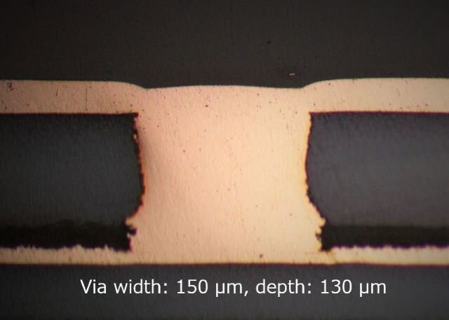
激光钻孔的孔壁呈锥形,纵横比超过 1:1 时电镀铜无法可靠覆盖孔底,导致开路。孔径 ≥ 介质层厚度,建议设计时留 15%~20% 余量。
叠孔设计需在图纸中明确标注 IPC-4761 Type VII 铜填孔 + 电镀盖帽规范,否则在热循环测试中可能出现孔铜断裂。
盘中孔(VIPPO)若不做平整化处理,焊接时会产生空洞或立碑。需标注平整度要求,如 ±10 μm。
HDI 积层应围绕芯板镜像对称,不对称叠层会导致板翘曲超标(常规要求 ≤ 0.75%,高精度 SMT 建议 ≤ 0.5%),影响后续装配。
阻抗值由线宽、介质厚度与材料 Dk 共同决定。高频项目建议在投板前提供仿真叠层,明确各层介质厚度与 Dk / Df,避免打样后反复调线宽。
速率达到 10 Gbps 以上时,未使用的过孔短桩(stub)会引入反射与插损。需在图纸中标注背钻层、深度与残留短桩要求(常规 ≤ 0.20 mm)。
从设计评审到成品出货,HDI 关键工序在洁净车间内完成,顺序层压与激光钻孔全程数据化管控。
解析 Gerber / ODB++,输出可制造性分析,确认阶数、叠层与盲埋孔方案。
依应用场景选定 FR4 / 无卤 / 罗杰斯材料,锁定来料批次与关键参数。
无菲林对位,实现 0.075 mm 级精细线路曝光,提升线路精度与一致性。
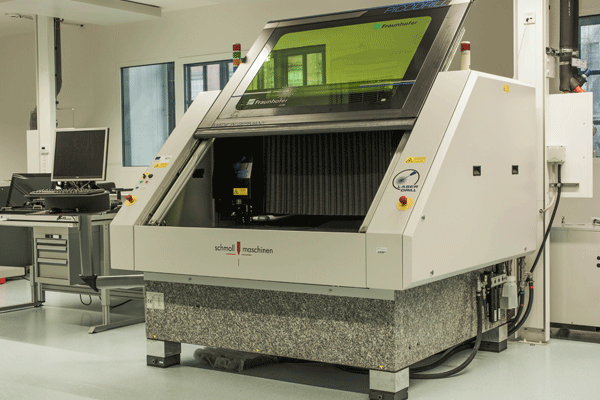
UV / CO2 激光成孔,量产标准 0.10 mm、打样极限 0.075 mm,支持叠孔与错孔。
全板电镀 + 图形电镀,叠孔与盘中孔按 IPC-4761 规范做填孔与盖帽。
HDI 特有工艺,多次压合逐层构建积层结构,层间对位精度严格管控。
ENIG / OSP / 沉银 / 沉锡等处理,保证焊盘可焊性与长期可靠性。
AOI + 飞针及治具电测 + X-ray 检测,附检测报告与 TDR 阻抗数据出货。
图形转移与钻孔区在万级环境完成,其余工序十万级,控制微尘与缺陷率。
自动光学检测叠加飞针与治具电测,覆盖开短路、线路缺陷等关键项。
对盲孔、叠孔与填孔质量进行 X-ray 与金相切片验证,确保互连可靠性。
可提供热冲击、TCT、HAST、HTS 等项目,出货附阻抗与切片测试数据。
MOQs, lead times, and pricing structures vary depending on the stage of the process, so be sure to understand these details before deciding where to start.
了解成本构成可以减少来回沟通,也方便您在设计阶段就做出取舍。
资料越完整,越容易一次确认阶数、叠层和工艺风险。没有完整 Gerber 时,也可以先用关键参数做预评估。
以下是客户在HDI打样与量产咨询中最常提出的问题,如需进一步确认请直接联系工程团队。
一阶 HDI(1+N+1):一次激光钻孔形成盲孔,一次层压循环,适用于 0.5 mm pitch BGA 出线。
二阶 HDI(2+N+2):两次激光钻孔,两次层压循环,适用于 0.4 mm pitch BGA。
三阶 HDI(3+N+3):三次激光钻孔,三次层压循环,适用于 0.3 mm pitch BGA,属打样极限能力,量产需评审。
任意层 HDI(ELIC):每一层都通过激光钻孔互连,适用于 0.3 mm pitch 以下 BGA,需专项评估。
选型原则:看 BGA pitch。0.5 mm 选一阶,0.4 mm 选二阶,0.3 mm 选三阶,0.3 mm 以下考虑任意层。阶数越高布线密度越大,但成本和加工难度也相应增加,不建议过度设计。
Mass Production Capabilities是可以写进合同、在批量订单中稳定复现的口径:层数 4~16 层、阶数 1+N+1 / 2+N+2、线宽间距 0.075mm、激光盲孔 0.10mm、阻抗 ±10%。
打样·极限能力需要在具体叠层、图形分布与材料确认后判定:层数至 32 层、阶数至 3+N+3、线宽间距 0.05mm、激光盲孔 0.075mm、阻抗 ±7%。
两者区分开的目的是避免量产阶段出现预期落差。若设计要求接近极限值且需量产,建议在打样阶段同步做量产可行性评估。
任意层互联对激光孔径与层间对位精度要求最高,属于Special Assessment范畴,不按常规能力直接报价。
需要您提供:完整的叠层结构与层数、BGA pitch 与球数、目标激光孔径与对位精度要求、预期量产批量。 我们会结合当前激光钻孔能力(量产 0.10 mm / 打样 0.075 mm)与顺序层压的对位累计公差给出可行性结论。
如果评估后判定当前制程无法稳定满足,我们会明确告知,而不是先接单再改设计。
支持。背钻用于去除高速过孔的残留短桩(stub),常规可控制在 0.20 mm 以内,需在图纸中标注背钻层、深度与残留要求。
盘中孔(VIPPO)支持树脂塞孔 + 电镀盖帽与铜填孔两种方案,平整度可控制在 ±10 μm 以内。 叠孔结构建议指定 IPC-4761 Type VII 铜填孔规范,以降低热循环下的孔铜断裂风险。
量产标准为 线宽间距 0.075mm / 0.075mm、激光盲孔 0.10mm、机械孔 0.20mm。
打样极限可到 线宽 0.05mm / 0.05mm、激光盲孔 0.075mm、机械孔 0.15mm,需评审确认。
精细线路依赖 LDI 激光直接成像实现。如果设计线宽低于 0.075mm,建议先提供 Gerber 做可制造性评估。
常规 HDI 打样交期为 5 to 8 business days;加急最快 72 小时,适用条件为一阶、≤ 8 层、标准叠层且排产允许。
The proofing stage typically 5 to 20 pieces即可启动,小批量试产建议 50 ~ 500 片,量产订单依叠层与批量排产报价。打样费在后续量产订单中可按规定抵扣,具体规则请在询价时确认。
Stacked Via:上层盲孔与下层盲孔在同一位置垂直堆叠,布线密度高,但每次层压后需精确对位并做填孔电镀,加工难度大、成本更高。
Staggered Via:上下盲孔错开位置,不垂直堆叠,无需填孔电镀,工序更少、交期更短,但占用空间较大。
我们支持二阶及以上叠孔设计(需评审),同时支持全阶数错孔设计。如果空间允许,建议优先采用错孔设计以降低加工风险与成本。
To provide an accurate quote, please provide the following information:
1. Gerber or ODB++ files(Required)
2. Layered Structure and Number of Layers Requirements(含阶数要求)
3. Substrate and Surface Treatment Requirements(FR4 / 无卤 / 罗杰斯、ENIG / OSP 等)
4. 盲埋孔设计要求(错孔 / 叠孔 / 盘中孔、是否背钻)
5. 阻抗要求与叠层仿真文件(高速项目)
6. 数量与交期要求
If you don't have the complete drawings yet, you can still provide参数需求(层数、阶数、线宽、尺寸、数量),我们可先给出参考价格区间。
普通多层板:机械钻孔通孔互连,最小线宽约 0.15mm、孔径约 0.3mm,适用于工控、电源等通用场景。
HDI Board:激光钻孔盲埋孔 + 积层结构,量产线宽 0.075mm、打样至 0.05mm,激光孔径 0.075~0.10mm,适用于手机、服务器、车载等小型化高密度场景。
IC Substrate:精度要求更高(线宽 15~20μm 级),用于芯片封装级别,制造难度与成本显著高于 HDI。
简单理解:HDI 是"板级高密度互连",IC 载板是"芯片级封装互连",两者应用场景与精度要求不同。
量产阻抗公差为 ±10%, Prototypes can be produced ±7%,支持单端与差分阻抗设计,出货可随附 TDR 时域反射测试报告与切片、膜厚数据。
对于 5G 通信、PCIe 5.0/6.0 等高速应用,建议在设计阶段就与工程团队沟通叠层方案与材料选型,必要时提供仿真叠层,以便提前锁定介质厚度与线宽。
Sure.我们支持在收到图纸前先签署保密协议,也接受贵司版本的 NDA 模板;如您还没有模板,可向业务窗口索取我方标准版本。
内部流程上,客户图纸仅用于工程评估与报价,参与人员限定在项目所需范围内,项目结束或终止后可依申请删除相关文件。
可以验厂。我们配合客户进行供应商审核与现场验厂,可提前提供体系文件、工艺流程与检测能力清单,审核后按整改项反馈并跟进闭环。
交付形式支持单板与拼板(邮票孔 / V-cut),出货采用真空防静电包装,附干燥剂与湿度指示卡,外箱标注批次号与追溯码,便于来料检验与问题追溯。
Fill out the form on the right or send your information directly to one of our engineers. Once we receive your information, we will first conduct a manufacturability assessment, and then provide you with a detailed quote and delivery schedule—the assessment itself is free of charge.
Gerber / ODB++、叠层、板厚、材料、盲埋孔结构、阻抗、表面处理、数量与目标交期。资料暂不完整时,也可先提交 BGA pitch、层数和关键线宽/孔径做预评估。
Fields marked with * are required. You may submit your parameter requirements even if you do not have drawings.