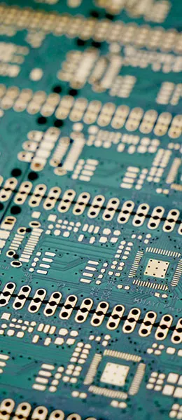
With the miniaturization and multifunctionality of electronic devices, as well as rapid advances in electronic packaging technology, the design and manufacturing of printed circuit boards (PCBs) are continuously evolving toward higher density, greater precision, and improved reliability, as well as narrower spacing, finer lines, and microvia technology. This trend poses greater challenges for PCB manufacturing technology, particularly in the production of precision patterns. This article will delve into the requirements of printed circuit board manufacturing technology and analyze the associated difficulties and challenges.

1. Let’s start by defining exactly what a “high-resolution PCB” is.
In the context of PCBs, “high resolution” does not refer to clarity, but rather toMinimum Line Width That Can Be Stably Reproduced After Pattern Transfer and Etching, and Its Consistency. It is determined by three factors:
- Minimum Line Width / Line Spacing (L/S): How fine a line can be produced, and how narrow a gap can be left between lines. In the industry, 3/3 mil (approximately 75/75 μm) is considered standard capability; 2/2 mil (50/50 μm) falls into the high-resolution range; and 1/1 mil (25/25 μm) represents the capability threshold requiring specialized processes and equipment.
- Line Width Tolerance: The deviation of the actual line width from the design value. High resolution isn’t about “being able to produce a 50 μm line,” but rather “mass-producing 1 million 50 μm lines, with 99% or more falling within ±10%.”
- Edge Quality: Check whether the edge is straight, whether there are any jagged edges (rat teeth), and whether there is any residual copper or over-etching. The quality of the edge directly determines impedance consistency and withstand voltage reliability.
If you break these three points down, it becomes clear that the challenge with high resolution has never been “getting it right the first time,” but ratherConsistently produced under conditions of large-volume, multi-batch production. Mass-production yield is the real hurdle.
2. Technical Requirements for Printed Circuit Boards
To manufacture high-quality printed circuit boards, especially when high-density and fine-line patterns are required, a series of technical requirements must be met. These requirements include:
2.1 Wire pitch: 0.40 mm
2.2 Inner-layer conductor: 0.05 mm
2.3 Outer Conductor: 0.05–0.0762 mm
2.4 Inner Copper Layer Thickness: 10 µm
2.5 Number of floors: 10–20
2.6 Filling Thickness: 0.05–0.127 mm
2.7 Blind Holes and Buried Holes: 0.05–0.20 mm
These technical requirements necessitate highly precise graphic production to ensure both high product quality and reliability, while also maintaining high production efficiency and low manufacturing costs. To achieve this goal, we need to thoroughly analyze the technical challenges involved in producing precision graphics and identify ways to improve the success rate.
To provide a clear picture of where these parameters fall on the industry capability spectrum, the following table compares common tiers:
| Ability Levels | Minimum Line Width/Spacing | Thickness of the inner copper layer | Microporous Pore Size | Typical Applications |
|---|---|---|---|---|
| General | ≥100 μm (4/4 mil) | 18–35 μm | ≥0.25 mm (mechanical drill) | Home Appliances, Industrial Control, Power Supplies |
| Advanced | 75 μm (3/3 mil) | 12–18 μm | 0.15–0.20 mm | Consumer Electronics Motherboards, Networking Equipment |
| High Resolution | 50 μm (2/2 mil) | 9–12 μm | 0.075–0.15 mm (laser) | Smartphones, Wearables, 5G Modules |
| Extreme | 25–40 μm (1/1.5 mil) | 5–9 μm (ultra-thin copper foil) | 0.05–0.075 mm | IC carrier substrates, advanced packaging substrates |
These technical requirements necessitate highly precise graphic production to ensure both high product quality and reliability, while also maintaining high production efficiency and low manufacturing costs. To achieve this goal, we need to thoroughly analyze the technical challenges involved in producing precision graphics and identify ways to improve the success rate.
These seven parameters are not isolated; they influence one another: the pitch determines the upper limits for line width and spacing; the copper thickness determines the minimum line width that can be reliably fabricated; the dielectric thickness determines the impedance and interlayer withstand voltage; and the via diameter determines whether mechanical drilling or laser drilling is used. In particular, once microvia diameters enter the 50–200 μm range, mechanical drilling is no longer sufficient, and laser drilling must be used instead. For a complete interconnect process flow, please refer toHDI (High-Density Interconnect) Circuit Boards。
To provide a clear picture of where these parameters fall on the industry capability spectrum, the following table compares common tiers:

3. Layout: From design data to physical traces on the copper foil
Regardless of the final line width, the outer-layer traces all pass through the same main link; understanding this link is key to identifying where the bottleneck lies:
- Preprocessing: Grind or micro-etch the board to remove oxidation and contaminants from the copper surface, while creating a microscopic roughness to ensure the adhesion of the photoresist.
- Coating: Apply the photosensitive resist to the copper surface (by roller coating, spray coating, curtain coating, or applying a dry film).
- Exposure: A design pattern is projected onto the photoresist using ultraviolet light, causing a photochemical reaction in the exposed areas.
- Development: Use developer to dissolve the unreacted (or reacted, depending on whether the image is positive or negative) areas, exposing the copper to be etched.
- Etching: The exposed copper is dissolved by the etching solution, while the copper beneath the resist is left intact to form the circuit.
- Film Removal: Remove the remaining photoresist to reveal the final circuit.
Of these six steps,Coating uniformity determines thickness consistency; exposure determines pattern accuracy; development determines edge steepness; and etching determines the final line width.. If any step gets out of control, the effects will be magnified later in the process. For specific parameter controls during the etching stage, seeA Detailed Explanation of the Etching Process in PCB Manufacturing。
4. Image Formation and Distortion
During the image formation process, the use of high-quality film, a thin photosensitive resist layer, and ultra-thin copper foil is critical to ensuring the high quality of the circuit patterns. However, image distortion is a common problem that can lead to inaccurate trace widths. For example, if a trace width is allowed to increase to 0.05 mm within a 0.05 mm spacing, short circuits can easily occur. Image distortion is typically associated with the surface condition of raw materials and quality defects during the manufacturing process. Issues such as pits, protrusions, and contamination can all reduce the adhesion of the photosensitive resist, resulting in circuit patterns that deviate significantly from the original design requirements.
If we break down the above passage into actionable troubleshooting steps, the causes of image distortion can generally be categorized into five types:
| Sources of Distortion | Performance | Root Cause | Countermeasures |
|---|---|---|---|
| Film Defects | Broken lines, jagged edges | Scratches on the film, specks of dirt, and dimensional drift due to temperature and humidity | Switch to LDI (Laser Direct Imaging) and eliminate the use of physical film |
| Condition of the Copper Surface | Some lines are too thin or broken | Dents, bumps, oxidation, fingerprints | Enhance pretreatment to control brush marks and micro-etching on the grinding plate |
| Uneven Coating | Systematic Deviation in Line Width Within a Board | Inconsistent photoresist thickness and varying exposure latitude | Switch to spray or roller coating, and monitor the wet film thickness |
| Exposure Deviation | The overall line width is too thick or too thin | Exposure Energy Drift, Alignment Offset | Perform daily Stouffer bar calibration |
| Incomplete development | Residual adhesive between wires causes a short circuit | Insufficient developer concentration, temperature, or spray pressure | Monitor the breakpoint at 40–60% |
5. Measure changes in the image
After image transfer, we can measure changes in the circuit pattern. By measuring variations in line width and spacing, we can evaluate differences between individual lines during the manufacturing process. The curve representing these image changes quantifies the frequency of variations in line width and spacing. Analysis of the Modulation Transfer Function (MTF) indicates that the quality of the circuit pattern is directly related to the processing characteristics. When the MTF and image quality level drop below 1, the calculated frequency of paired lines is referred to as the breakage frequency, indicating that the lines are in a state between reliable and unreliable processing. To improve the reliability of the output, it is essential to implement the fewest possible yet most effective process steps.
This section discusses how to use statistical methods to quantify graphical capabilities. In production environments, this is typically done as follows:
- Sampling: Take one set of line width/spacing samples at each of the four corners and the center of the board, with each set containing at least 30 lines; avoid using only data from the edges of the board.
- Measurement: Measure the wire using a wire width gauge or a cross-section microscopeTop Width与Bottom Width, and the difference between the two reflects the degree of side etching.
- Statistics: Calculate the mean and standard deviation, and use Cpk to measure process capability. High-resolution production lines generally require a line width Cpk of ≥ 1.33.
- Differences in Judgment: A bimodal distribution indicates the presence of two types of systematic deviations (typically due to uneven exposure or coating), while a long tail indicates the presence of random defects (typically related to cleanliness or the copper surface).
Deviations in line width not only affect appearance but also directly alter impedance and current-carrying capacity; the quantitative relationship between the two is shown inRelationship Between PCB Trace Width and Current。
6. Changes in Raw Materials for the Production of Fine-Line Circuit Patterns
The key to achieving high-yield, high-resolution circuit patterning lies in selecting the correct photoresist. The photoresist is a critical factor in image formation. New process equipment, enhanced process control, and the skilled expertise of the staff also play a crucial role in achieving high-quality circuit patterning. Currently, roller coating and spray coating are the primary methods used to manufacture high-density PCBs. However, these methods require significant investment and still present challenges in terms of reliability. In particular, for the fabrication of fine-line patterns, liquid photoresists are not necessarily a completely reliable or feasible process technology.
The three variables on the raw material side often have a greater impact on resolution than those on the device side:
- Copper Foil Thickness and Contour: The thinner the copper foil and the lower its surface roughness (Rz), the less side etching occurs during etching. Conventional electrolytic copper foil has an Rz of approximately 5–8 μm, while ultra-low-profile copper foil (VLP/HTE) can achieve 2–3 μm, which is a prerequisite for producing lines narrower than 50 μm. For detailed selection guidelines, seePCB Materials。
- Resist Thickness: The thinner the photoresist, the smaller the effects of diffraction and scattering during exposure, and the higher the resolution. However, if it is too thin, it can lead to pinholes and reduced etch resistance. In actual production, dry films are typically 15–25 μm thick, while the coating thickness of liquid photoresists is controlled at 8–15 μm.
- Dimensional Stability of the Substrate: Expansion and contraction of the laminated panels after lamination can directly cause alignment errors. High-resolution panels typically require the substrate to undergo a pre-baking process to limit expansion and contraction to within 100 ppm.
7. High-Throughput, High-Resolution Photoresist Technology
When creating circuit patterns, selecting the right photoresist is crucial. The quality of the photoresist directly affects the quality of the image. By controlling the exposure light source and fully utilizing the high resolution of the photoresist, it is possible to improve the yield of fine-line fabrication. UsingHDIThe (Hot Development Inhibition) process can increase the contrast of the photoresist, thereby improving resolution. The basic principle of HDI is to immerse the exposed film in hot water, which helps enhance the hardness and stability of the photoresist. However, further research and development are needed to determine whether the HDI process is suitable for all photoresists.
It should be noted that, in the current PCB industry terminology,The more common meaning of HDI is High Density Interconnect., refers to an interconnect structure characterized by micropores, fine lines, and thin dielectric layers; the term “Hot Development Inhibition” mentioned above is used in specific process literature to refer to a processing technique that enhances photoresist contrast through heat treatment. Although the two terms share the same abbreviation, their meanings differ; when reading materials, be sure to distinguish between them based on context. For a complete high-density interconnect process flow, please refer toA Comprehensive Analysis of the HDI PCB Manufacturing Process。
The practical differences between the two technical approaches for photoresists:
| Comparison Items | Dry Film Photoresist | Liquid Photoresist (Liquid / LPI) |
|---|---|---|
| Coating Method | Hot-Roll Laminating Film | Roll Coating / Spray Coating / Band Coating |
| Thickness Uniformity | Okay, the thickness is determined by the membrane material. | Due to the coating equipment, there is a slightly greater variation within the panel. |
| Filling Capacity | Poor; insufficient filling of surface depressions can easily cause bubbles. | Okay, it can adhere to irregular surfaces. |
| Resolution | Due to film thickness limitations, stability is generally achieved at 50 μm or more. | Can be applied in thinner layers, down to 25–30 μm |
| Capital Expenditures | 低 | High (Coating Line + Cleanroom) |
| Applicable Scenarios | Standard Boards, Inner Layers, High-Volume Production | High-Resolution Outer Layers, Fine Pitch, HDI |
8. High-Density Image Resolution Processing Program
To reduce image distortion and produce conductors with a width of 0.10–0.15 mm, new manufacturing processes, such as HDI, must be adopted. The principle behind this process is to immerse the film in hot water after exposure to improve the resolution of the photoresist. This method reduces image distortion and ensures that the edges of the conductors are neat and free of deformation. The application of the HDI process increases the hardness of the resist after exposure, providing greater stability and helping to improve resolution.
On today's production lines, the mainstream approach to improving resolution has shifted from "post-processing enhancement" to "upgrading the exposure method"—that is, replacing traditional film exposure with LDI:

- LDI (Laser Direct Imaging): By using a laser beam to scan and image directly onto the photoresist according to the design data, the need for physical film is eliminated, thereby removing an entire category of defects—such as film warping, scratches, and dust spots—while also allowing for adjustments based on the actual expansion and contraction of the board surface.Real-Time Zoom Compensation, with positioning accuracy within ±10 μm.
- CCD Alignment Exposure System: It still uses film, but uses a CCD to automatically align the target, offering higher precision than manual alignment and lower costs than LDI; it is suitable for medium-resolution batch production.
- Traditional Manual/Semi-Automatic Exposure: Relies on manual alignment; suitable for standard boards with line widths of 100 μm or greater; yield rates are difficult to guarantee when producing fine lines.
For a detailed comparison of the three methods, seeA Comparison of LDI and CCD Exposure Systems. For information on process windows and capability boundaries, seePCB Manufacturing Capabilities。
9. The Etching Process: The Ultimate Determinant of Resolution
No matter how precise the exposure is, fine lines cannot be produced if the etching process is out of control. The key to etching isEtch Factor—The ratio of etch depth to lateral etch rate. The higher the etch factor, the steeper the line edges, and the better the design line width is maintained.
| Copper Thickness | Typical Etching Factors | Unilateral Drilling and Erosion Volume | Stable Minimum Line Width |
|---|---|---|---|
| 5 μm (ultra-thin) | 4.0–5.0 | 1.0–1.3 μm | 25 μm |
| 9 μm (1/4 oz) | 3.0–4.0 | 2.3–3.0 μm | 40 μm |
| 18 μm (1/2 oz) | 2.5–3.0 | 6.0–7.2 μm | 75 μm |
| 35 μm (1 oz) | 2.0–2.5 | 14–17.5 μm | 100 μm |
| 70 μm (2 oz) | 1.5–2.0 | 35–46 μm | 200 μm |
This table explains why thin copper is used in almost all high-resolution boards:If the copper thickness is halved, the line width can generally be halved as well.. For the three key control points in the etching process, seeThree Key Points of the PCB Etching ProcessFor specific techniques on line width and spacing, seeAnalysis of Techniques and Challenges in Precision PCB Line Width and Spacing。
10. Verification: How to Confirm That It Was Actually Done
High-resolution boards cannot rely solely on visual inspection of finished products; checkpoints must be established at three key stages:
- AOI (Automated Optical Inspection): After etching, perform a full-board scan to detect short circuits, notches, copper residue, and pinholes. For fine-line boards, the AOI system requires higher pixel resolution, and detection thresholds must be set individually based on line width.
- Line Width Measurement: For each batch of random inspections, record the top/bottom line widths and Cpk; if any abnormal trends are detected, stop the machine and make adjustments.
- Microsection: Measuring the copper thickness, dielectric thickness, copper thickness on the hole walls, and wire edge morphology of the cross-section under a microscope serves as the ultimate basis for determining whether the process truly meets the specifications. Key points for observing micro-sections are outlined inKey Points for PCB Reliability and Microsection Inspection。
- Electrical Testing: Perform a comprehensive open-circuit and short-circuit test. The risk of open circuits and short circuits in fine-pitch circuit boards is significantly higher than in standard boards, so this step cannot be skipped.

11. Balancing Cost and Yield

With each increase in resolution, costs rise exponentially rather than linearly. When selecting a model, you must strike a balance among the following four factors:
- Copper Foil Grades: Ultra-low-profile copper foil costs 1.5–2.5 times as much as standard copper foil.
- Exposure Methods: The capital investment for LDI equipment is 3–5 times that of traditional exposure systems, and its throughput is lower than that of film-based systems using parallel exposure.
- Resist Process: Liquid photoresists require coating lines and a higher level of cleanliness.
- Yield Loss: The thinner the wire width, the higher the open-circuit and short-circuit defect rates, leading to increased rework and scrap costs.
The best practices are as follows:Set the level based on the tightest spot, not on the entire board.: Since only the BGA lead-out area on the entire board requires a 50 μm trace width, while 75 μm is sufficient for the rest of the board, the process should be set to 50 μm but strictly controlled only in the specific area to avoid overprocessing the entire board. For stability requirements for multilayer high-resolution boards, seeStability and Reliability of Multilayer PCBs。
12. Conclusion
Printed circuit board manufacturing technology faces significant challenges in the pursuit of high density, high precision, high reliability, and miniaturization. Image formation and distortion, variations in measurement images, fluctuations in raw materials, and photoresist technology are all critical issues that must be addressed when producing precision patterns. By adopting new process methods such as HDI, it is possible to increase yield and resolution, thereby better meeting the manufacturing demands of high-density PCBs.
In PCB manufacturing, to maintain high quality and reliability, manufacturers must continuously research and improve their processes to meet ever-changing technical requirements. Only through scientific analysis and innovative process methods can the successful production of high-density, fine-line patterns be achieved.
Frequently Asked Questions
1. What is the HDI process?
The HDI (Hot Development Inhibition) process is a manufacturing method used to produce high-density circuit patterns. It improves the resolution of the photoresist by immersing the exposed film in hot water, thereby achieving higher yields and resolution.
2. Why is the choice of photoresist so important?
The photoresist directly affects the quality of the circuit pattern. Selecting the appropriate photoresist can improve resolution and pattern stability.
3. Why is precision graphic production so important?
Precision pattern fabrication is a critical step in the manufacturing of printed circuit boards, as it directly affects the performance and reliability of the boards. Only through precise pattern fabrication can the demands of modern electronic devices for high-density PCBs be met.
4. What factors can cause image distortion?
Image distortion may be related to the quality of raw materials, quality defects during the manufacturing process, and the performance of the photoresist.
5. How can I improve the resolution of a circuit diagram?
The use of new manufacturing processes, such as HDI, can improve the resolution of circuit patterns; at the same time, it is necessary to select an appropriate photoresist and control the exposure light source.
6. When designing a 50 μm line width, what copper thickness should be selected?
Preferably, use inner-layer copper foil that is 9 μm (1/4 oz) or thinner. The thicker the copper, the more severe the lateral etching; if a 50 μm trace width is used with 35 μm copper, the trace edges will be severely slanted or even open. If structural strength requirements necessitate the use of thick copper, the trace width should be increased to 100 μm or more.
7. How is LDI better than film exposure?
The key advantage is the elimination of physical film, which removes defects such as warping, scratches, and specks. It also enables real-time scaling compensation based on the actual expansion and contraction of the board surface, improving alignment accuracy from the ±50 μm range to the ±10 μm range. The drawbacks include high equipment costs and longer exposure times per board.
8. How is the etching factor calculated, and what value is considered acceptable?
Etching factor = etching depth ÷ single-sided etch-through. For standard boards, a value of ≥2.0 is acceptable; for high-resolution boards, ≥3.0 is required; and for ultra-fine lines (≤30 μm), ≥4.0 is required. When the etching factor is below 2.0, the line edges will take on a noticeably trapezoidal shape, causing both impedance and current-carrying capacity to deviate from the design specifications.
9. Why are fine-line circuit boards more prone to open circuits?
There are three reasons: First, a large proportion of the etching is lateral, and the line width margin is small; second, even tiny pits on the copper surface or pinholes in the photoresist can cause line breaks in fine lines; third, the etching solution is not sufficiently circulated, resulting in inconsistent etching rates between dense and sparse areas (pooling effect).
10. Should high-resolution capabilities be specifically verified during the procurement process?
Yes. The “minimum line width” specified by PCB manufacturers is often the limit for prototyping and does not reflect their mass production capabilities. When purchasing, you should clarify three things: the minimum line width and line spacing for mass production, line width tolerances or Cpk requirements, and the corresponding copper thickness and inspection methods. The five key requirements for manufacturing are outlined in5 Key Requirements and Optimization Strategies for the HDI Manufacturing Process。
Related Recommendations:Stability and Reliability of Multilayer PCBs · 5 Key Requirements and Optimization Strategies for the HDI Manufacturing Process