

Printed circuit boards play a crucial role in modern electronics manufacturing, and electroplating is one of the key processes involved. Different types of PCB electroplating can meet a wide range of needs, but they also contribute to the diversity of the PCB market. This article will provide an in-depth look at the various types of PCB electroplating and their applications.
1. First, identify the issue: What problem does surface treatment address?
Copper is the ideal metal for interconnects, but it has one fatal flaw—It oxidizes when exposed to air, and copper oxide is not weldable.. The entire purpose of surface treatment (Surface Finish) is to seal the bare copper with a thin protective layer prior to final soldering, while ensuring that this protective layer can be easily displaced or dissolved by the solder during the soldering process.
Mainstream surface treatments can be divided into two broad categories based on whether they contain gold, and the applications for each category differ significantly:
| Process | Typical Thickness | Flatness | Service Life | Solderability | Relative Cost |
|---|---|---|---|---|---|
| HASL Tin Plating (Lead-Containing) | Sn 1–15 μm | 差 | 12 months | 优 | 1× |
| HASL Lead-Free Solder Paste | Sn 1–15 μm | 差 | 12 months | 良 | 1.1–1.3× |
| OSP Organic Solder Protection Film | 0.2–0.5 μm | 优 | 6 months | Good (decreased after one reflux) | 1.2–1.5× |
| Tin Plating / Silver Plating | 0.1–1.2 μm | 优 | 6–12 months | 良 | 1.8–2.5× |
| ENIG Chemical Gold Plating | Ni 3–6 μm / Au 0.05–0.1 μm | 优 | 12 months+ | 优 | 2.5–3.5× |
| ENEPIG | Ni 3–6 / Pd 0.05–0.15 / Au 0.03–0.1 μm | 优 | 12 months+ | Premium (can be accented with gold thread) | 3.5–5× |
| Hard Gold Plating (Gold Fingers) | Ni 3–6 μm / Au 0.5–1.5 μm | 优 | 24 months+ | Excellent (Wear Resistance) | 4–8× (local) |
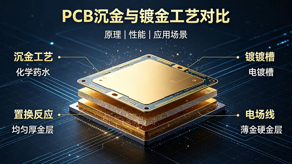
2. Full-board gold plating
Full-board gold plating is a common type of printed circuit board plating, which includes gold plating, nickel-gold plating, electrolytic gold plating, electroplated gold, and electroplated nickel-gold plating. These processes involve dissolving nickel and gold in a chemical solution, then immersing the circuit board in an electroplating tank to deposit a nickel-gold plating layer on the copper foil surface through an electrical current. Electrolytic nickel-gold plating is widely used in electronic products due to its high hardness, wear resistance, and resistance to oxidation.
3. Gold Inlay
Shen JinThis is a type of electroplating in which a coating is formed through chemical redox reactions. Typically, the gold layer produced by electroless gold plating is thicker; this is a type of chemical nickel-gold metal deposition method. Electroless gold plating is generally used in applications that require a thicker gold layer, which is why this process is often referred to as electroless gold plating.
Here, it’s important to clarify a key engineering point; otherwise, it’s easy to make the wrong choice during the selection process:The layer of gold in dip-plated gold is actually much thinner than that in electroplated gold.. The gold layer in ENIG is typically only 0.05–0.1 μm (2–4 μin) thick, and its purpose is to protect the underlying nickel layer from oxidation; In contrast, the gold layer in hard gold plating can reach 0.5–1.5 μm (20–60 μin)—a difference in thickness of one order of magnitude—which is why hard gold can withstand the wear and tear of repeated insertion and removal. The real difference between the two lies inDeposition Mechanism与Crystal Structure...rather than ”which one is thicker.” For a detailed breakdown of the technical principles, seeENIG Production Process and Its Advantages and Disadvantages。
4. Gold-plated circuit boards
With the advancement of integrated circuits, the number of IC pins has increased, and traditional vertical tin-spraying processes struggle to ensure that small pads are evenly coated, posing challenges for surface-mount technology. In addition, tin-sprayed circuit boards have a relatively short shelf life. Gold-plated circuit boards were developed to address these issues:
- In surface-mount technology, particularly for ultra-small surface-mount components, the flatness of the pads directly affects the quality of the solder paste printing process, which in turn affects the quality of the subsequent reflow soldering.
- During the prototyping phase, circuit boards often have to sit unused for weeks or even months, and gold-plated circuit boards have a much longer shelf life than lead-tin alloy boards, making them a popular choice.
However, as circuit layout has become increasingly dense, trace widths and spacing have shrunk to 3–4 mils, leading to the problem of gold wire short circuits. Furthermore, as signal frequencies increase, signal transmission through multilayer boards has a greater impact on signal quality. This phenomenon is known as the skin effect, whereby high-frequency alternating current tends to concentrate on the surface of the conductor.
5. Immersion Gold Circuit Board
To address the aforementioned issues with gold-plated circuit boards, people have begun using electroless gold-plated circuit boards, which have the following characteristics:
- Gold plating and gold-plated finishes form different crystal structures, resulting in a more yellow appearance that better meets customer requirements.
- The crystal structure of sintered gold is relatively dense, making it easy to weld; it does not cause welding issues, thereby reducing customer complaints.
- In immersion-gold printed circuit boards, gold is plated only on the pads, so the skin effect has a minimal impact on signal transmission.
- Electroplated gold circuit boards have a denser crystal structure and are less prone to oxidation.
- Since the metal layer on an immersion gold PCB is limited to the pads, gold wire short circuits do not occur.
- The solder mask on an embedded gold PCB bonds more securely to the copper layer.
- Immersion gold circuit boards do not affect the spacing between traces.
Overall, gold-plated circuit boards are a type of electroplating that meets the demands of modern electronics manufacturing. Not only do they have an attractive appearance, but they also perform exceptionally well in terms of signal transmission and soldering.
6. Comparison of the Principles Behind the Two Processes

When you compare gold-plated and gold-filled items side by side, the difference is immediately apparent:
| Comparison Items | Electrolytic Nickel-Gold Plating (Electrolytic Ni/Au) | Electrolytic Nickel Immersion Gold (ENIG) |
|---|---|---|
| Deposition Mechanism | When an external current is applied, metal ions are reduced at the cathode. | Self-catalyzed chemical redox reaction; no power supply required |
| Is a conductive path required? | Yes, the circuits on the entire board must be electrically connected. | No, isolated pads can also be gold-plated. |
| Coating Range | Full-board conductor (requires leads; to be etched and severed later) | Areas where only the copper pads are exposed |
| Gold Layer Thickness | 0.5–1.5 μm (thicker versions available upon request) | 0.05–0.1 μm (subject to process limits) |
| Nickel Coating Thickness | 3–6 μm | 3–6 μm |
| Crystal Structure | Columnar, dense but with internal stress | Layered, phosphorus-containing, and more compact in structure |
| Thickness Uniformity | Due to the current distribution, the edges are thicker and the center is thinner. | Chemical deposition, good uniformity |
| Cost | Gold is used in large quantities and is expensive. | It uses very little gold and is low-cost. |
The production line steps for the two processes are as follows:
- Electroplated Nickel-Gold: Pretreatment (degreasing, micro-etching, activation) → Nickel plating (Watt nickel or aminosulfonic acid nickel) → Rinsing → Gold plating (acidic gold or cyanide gold) → Rinsing → Drying → Etching to sever the plated leads.
- ENIG: Pretreatment (degreasing, micro-etching, activation) → Chemical nickel plating (reduction with hypophosphite, with concurrent precipitation of phosphorus) → Water rinse → Chemical gold plating (displacement reaction, in which gold displaces nickel from the surface) → Water rinse → Drying.
”Among them"Is a conductive path required?“This is the most fundamental difference between the two in terms of process. For electroplated gold, the conductors on the entire board must be electrically connected in order to carry current; this often requires the additional routing of ”electroplating leads” during design, which are then etched away after plating—a significant burden in fine-pitch designs. ENIG relies on chemical deposition and does not have this issue; this is the fundamental reason why it has completely replaced electroplated gold on high-density boards. For detailed differences between the two, please refer toThe Difference Between Electroless Nickel-Gold and Electrolytic Nickel-Gold。

7. Gold-Wire Short Circuits and the Skin Effect: Why High-Density Boards Have Moved Away from Electroplated Gold
The two issues mentioned in the original text are critical when it comes to high-density fiberboard:
7.1 Gold Wire Short
Electroplating deposits a layer of gold on all exposed conductors, including the sides of the traces. When the line width and spacing are reduced to 3–4 mil (75–100 μm), the edges of the gold layer remaining after etching formSlender metal strands (slivers)...These could potentially spill over during subsequent processes and bridge adjacent traces, causing a short circuit. ENIG is deposited only on the pads; there is no gold layer on the sides of the traces, which eliminates this problem in principle.
7.2 Skin Effect
High-frequency alternating current tends to flow near the surface of a conductor. The higher the frequency, the thinner the surface layer where the current is concentrated—the skin depth of copper is approximately 2.1 μm at 1 GHz and approximately 0.66 μm at 10 GHz. This means thatThe current in high-frequency signals flows primarily within the outermost few micrometers of the conductor.. With electroplated gold, the entire surface of the trace is coated with a layer of gold and nickel, so the signal must travel near the nickel layer, which has a higher resistivity (approximately 7.0 × 10⁻⁸ Ω·m, four times that of copper), resulting in a significant increase in signal loss. ENIG applies gold plating only to the pads, while the surface of the traces remains copper, resulting in better high-frequency performance.
The skin depth of copper at several common frequencies, for easy estimation:
- 100 kHz: Approximately 0.21 mm — the skin effect does not need to be considered for thick copper plates.
- 1 MHz: Approximately 66 μm — 2 oz of copper (70 μm) is close to the critical limit.
- 1 GHz: Approximately 2.1 μm — at this point, the roughness of the copper foil begins to dominate the losses.
- 10 GHz: Approximately 0.66 μm — The surface treatment layer is part of the current path, and the plating material directly affects losses.
This is why RF boards and high-speed digital boards almost without exception opt for ENIG or other non-electrolytic gold plating processes, while hard gold plating is reserved only forGold-plated contacts that need to be repeatedly plugged in and unpluggedApplications involving this type of wear.
8. Pad Flatness and Shelf Life
Flatness is a critical factor for fine-pitch components. The tin layer thickness in Hot Air Solder Leveling (HASL) is uneven, with height differences between pads reaching 10–30 μm. For BGAs and QFNs with a pitch of 0.4 mm or less, this unevenness is sufficient to cause uneven solder paste deposition, leading to cold solder joints or short circuits. The surface roughness of ENIG is typically within 1–2 μm, making it the default choice for fine-pitch components.
In terms of shelf life, ENIG can last for more than 12 months under standard storage conditions (dry, sealed, and protected from sulfidation), while OSP lasts only 6 months and its performance degrades after a single reflow cycle. Although tin plating can also be stored for 12 months, it exhibits poor surface flatness.During the prototyping phase, when circuit boards are left unused for weeks or even months, ENIG is the most reliable option.—This is precisely why the original text mentioned that gold-plated boards were popular during the pilot production phase, and ENIG offers the same advantage at a lower cost.
Even the longest shelf life depends on proper storage. Key points for storing ENIG boards:
- Vacuum-sealed + desiccant, Use as soon as possible after opening; if left exposed for more than 24 hours, it is recommended to bake it.
- Avoid environments containing sulfur: Sulfur reacts with silver and copper to form sulfides; silver-plated plates are particularly susceptible to this reaction.
- Avoid direct contact with the pads: The salt and oils in fingerprints can stain the gold surface.
- First In, First Out: Batch Management: Boards that are more than 12 months old must undergo a re-test for solderability before soldering.
9. Selecting a Model Based on the Application
| Use Cases | Preferred Process | Alternatives | Reasons Not to Choose It |
|---|---|---|---|
| BGA / Fine-pitch (0.4 mm or less) | ENIG | ENEPIG | Insufficient tin plating flatness; OSP failure after multiple reflow cycles |
| Golden Finger / Repeatedly Plugging In and Unplugging | Hard Gold Plating (Partial) | Gold Plating + Spot Hard Gold Plating | The ENIG gold layer is too thin; it wears through after just a few dozen insertions and removals. |
| Gold wire bonding (COB/bonding) is required | ENEPIG | Soft Gold Plating | Insufficient adhesion between the ENIG nickel layer and the gold wires |
| High-frequency / High-speed (≥5 GHz) | ENIG or OSP | Sunk Silver | Electroplated gold causes signals to propagate near the nickel layer, resulting in increased signal loss. |
| Cost-sensitive, high-volume consumer products | Lead-Free Solder Plating / OSP | — | ENIG costs 2–3 times as much |
| Press-fit Connection | 喷锡 / OSP | ENIG | 硬金层太硬会影响压接区形变 |
| 车载 / 医疗高可靠 | ENIG / ENEPIG | — | OSP 与喷锡的长期可靠性不足 |
如果要在镀金与沉金之间做选择,判断路径很短:先看有没有插拔或打金线需求——有就用硬金(局部)或 ENEPIG;没有就选 ENIG,它在平整度、待用寿命、高频特性、成本四项上综合最优。更细的选型逻辑见如何选择镀金或沉金表面处理,四种常见工艺的横向对比见4 Common PCB Surface Treatments。

10. 常见缺陷:黑盘与金脆
镀金类工艺有两个臭名昭著的失效模式,采购与品质都应了解:
| 缺陷 | 现象 | 根因 | Countermeasures |
|---|---|---|---|
| 黑盘(Black Pad) | 焊盘发黑,焊接后焊点强度极低、易脱落 | 沉金液对镍层过度腐蚀,形成富磷脆化层 | 控制金槽参数与浸金时间;改用 ENEPIG |
| 金脆(Gold Embrittlement) | 焊点发脆、强度下降 | 金溶入焊料超过 3 wt%,形成脆性的 AuSn₄ 金属间化合物 | 控制金层厚度;焊接前搪锡去金 |
| 镍层氧化 / 不上锡 | 焊盘变色、拒焊 | 金层太薄或有孔隙,镍层被氧化 | 提高金厚至 0.08 μm 以上;缩短存放时间 |
| 金面发白 / 污染 | 外观异常,可焊性下降 | 水洗不充分、有机物残留 | 加强水洗;改用垂直沉金线 |
| 金手指磨损露镍 | 插拔若干次后露出镍层 | 金层厚度不足或硬度不够 | 硬金加厚到 0.76 μm(30 μin)以上 |
Among them黑盘是最麻烦的一种——它在外观上可能完全正常,只有焊接后做拉力测试或切片才会暴露,一旦批量发生,损失极大。因此高可靠项目通常要求板厂提供沉金药水的参数管控记录与周期性切片报告。沉金板氧化的分析与对策见PCB沉金板氧化问题分析与改善对策。

来料检验环节对镀金类工艺的常规检查项:
- Appearance:金面色泽均匀,无发黑、发白、水印、划伤。
- 金厚 / 镍厚:XRF 荧光测厚,按 IPC-4552 判定。
- Solderability:漂锡试验(235 ℃、2–3 s),润湿面积 ≥95%。
- 附着力:胶带试验,镀层不得脱落。
- 孔隙率:硝酸蒸汽试验或电化学法,评估金层致密性。
11. 结论
电路板电镀类型的选择取决于多个因素,包括应用需求、成本和性能。在选择电路板时,务必考虑您的具体需求,以确保选择了最适合的电镀类型。同时,了解各种电镀类型的特点将有助于您更好地理解电路板市场的多样性。
一句话总结选型:要插拔耐磨就用电镀硬金,要打金线用 ENEPIG,其余绝大多数场景 ENIG 是性价比最优解,成本极度敏感且无细间距时用喷锡或 OSP。具体工艺参数与能力清单见表面处理工艺能力。
Frequently Asked Questions
1. 为什么沉金电路板在高密度表面贴装工艺中更常见?
沉金电路板的焊盘平整度对于高密度表面贴装工艺的质量至关重要,因此它在这种应用中更常见。
2. 为什么沉金电路板在试制阶段更受欢迎?
沉金电路板的待用寿命比铅锡合金板长,这使得它在试制阶段更受欢迎。
3. 趋肤效应对电路板有什么影响?
趋肤效应会导致高频信号在导线表面集中传输,影响信号质量。
4. 沉金电路板和镀金电路板有什么区别?
沉金电路板和镀金电路板在晶体结构、焊接性能、待用寿命和信号传输方面存在区别。
5. 如何选择适合自己需求的电路板电镀类型?
选择电路板电镀类型应考虑应用需求、成本和性能,最好咨询专业制造商的建议。如果您需要更多信息,请随时与我们联系。
6. 沉金和镀金,到底哪个金层更厚?
镀金(电镀硬金)更厚,金层通常 0.5–1.5 μm;沉金(ENIG)只有 0.05–0.1 μm,差一个数量级。沉金里的”沉”指的是化学沉积方式,不是厚度。沉金的金层只起保护镍层不被氧化的作用,焊接时金会迅速溶入焊料,真正形成焊点的是下面的镍。
7. 3-4 mil 线距下为什么不能用整板镀金?
因为电镀金会沉积在走线侧面,蚀刻后残留的金层边缘会形成细长金属须(sliver),在后续工序中倾倒跨接到相邻走线,造成金丝短路。线距越小风险越高。ENIG 只在焊盘上沉积,走线侧面没有金层,从原理上避免了这个问题。
8. 金手指为什么一定要电镀硬金而不能用沉金?
因为插拔磨损。沉金的金层只有 0.05–0.1 μm,插拔几十次就会磨穿露出镍层,镍氧化后接触电阻急剧上升。电镀硬金厚度可达 0.5–1.5 μm 且硬度高(添加钴或镍的合金金),能承受数百到上千次插拔。常见做法是整板做 ENIG,再在金手指区域局部加镀硬金。
9. 什么是黑盘?怎么避免?
黑盘是 ENIG 特有的失效模式:沉金液对镍层过度腐蚀,在镍金界面形成富磷脆化层,外观可能正常但焊点强度极低、易脱落。避免办法是控制金槽参数(温度、pH、金浓度)与浸金时间,关键项目改用 ENEPIG(钯层能阻隔镍的过度腐蚀),并要求板厂提供参数管控记录与周期切片报告。
10. ENIG 的金层厚度要求多少合适?
IPC-4552 对 ENIG 的金层要求是 0.05–0.125 μm(2–5 μin)。太薄(<0.05 μm)镍层易氧化导致拒焊;太厚(>0.15 μm)会增加金脆风险,且成本上升。常规推荐控制在 0.08–0.10 μm,同时镍层保证 3–6 μm。
Further Reading:PCB沉金与镀金工艺原理 · 如何选择适合的SMT贴片机
