

Etching is a critical step in the PCB manufacturing process. This article provides a detailed overview of the etching process, with a particular focus on vacuum etching technology for PCBs, as well as its principles and advantages.
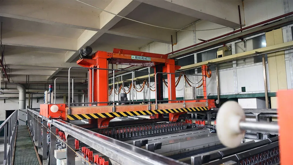
Basic Principles of the PCB Etching Process
In PCB manufacturing, etching is a critical step in forming circuit patterns and pads on the copper substrate according to design specifications. The basic principle is simple: the copper substrate is covered with a resist layer; the copper not protected by the resist reacts with the etchant and is etched away, ultimately forming the designed circuit patterns and pads.
Although the principle of etching seems simple, it presents many challenges in practical applications, particularly when producing fine circuits. These challenges mainly manifest in two ways: the etching results must be just right—neither too wide nor over-etched.
The Pool Effect in PCB Manufacturing
PCB manufacturers prefer to use horizontal etching lines in their production processes to maximize automation and thereby reduce costs. However, horizontal etching also has a drawback: the unavoidable “pooling effect.”
This phenomenon results in different etching effects on the top and bottom surfaces of the board, with the etching rate at the edges of the board being faster than that at the center. This unevenness can negatively impact the quality of the PCB, particularly in applications that require fine circuit patterns.
“The ”pooling effect” is caused by the uneven distribution of the etching solution on the board. In the areas near the edges of the circuit board, the etching solution flows out more easily, allowing for greater exchange between fresh and used solution, which helps maintain a consistent etching rate. In contrast, in the center of the board, the flow of the etching solution is restricted, leading to reduced etching efficiency and poorer etching results.
Even with the implementation of certain specialized production process controls and compensation methods—such as a spray system with horizontally adjustable nozzles independent of the transport direction, the addition of oscillating spray bars, and the inclusion of a corrective re-etching section—it remains difficult to effectively resolve the “pooling effect” issue.
The Emergence of Vacuum Etching Technology
To overcome the “pooling effect” and improve the quality and efficiency of etching, PILL e.K. introduced a new process technology at the end of last year known as vacuum etching technology. This technology uses a pump to extract spent etching solution, improving the flow of the solution on the upward-facing surface of the board and thereby preventing the “pooling effect.”
The principle behind vacuum etching technology is quite simple. In the etching section, in addition to the nozzles, evacuation units are installed between the nozzles at a relatively close distance from the surface of the circuit board. These evacuation units draw away the used etching solution, which is then returned to the module’s liquid reservoir via a closed loop.
The advantages of vacuum etching technology are primarily reflected in the following areas:
Improved Uniformity:
After vacuum etching, the etching results are very uniform across the entire surface. This helps ensure the quality of the PCB traces.
Increased Production Capacity:
Etching speeds have increased, production times have been reduced, and the yield of the etching process has improved.
Reduce rework:
Since a satisfactory result can be achieved on the first etching, there is no need to rework the part by etching it again.
Reduce Costs:
This has reduced the amount of related plant control engineering and lowered costs.
Wide Range of Applications:
Vacuum etching technology is suitable for producing ultra-fine conductors, eliminating the need to install a swiveling jet manifold.
Environmentally Feasible:
An environmentally friendly recycling system can be installed to reduce the discharge of chemical waste.
The Future of Vacuum Etching Technology
Vacuum etching technology shows tremendous potential and is particularly well-suited for the production of circuit boards with fine and ultra-fine conductor structures. Preliminary tests have already demonstrated that this technology is capable of producing conductive patterns smaller than 50 micrometers.
The capability to produce thick copper board circuits using vacuum etching technology is also undergoing further evaluation. Whether using traditional copper(I) chloride etching solutions or iron(III) chloride etching solutions, vacuum etching technology has demonstrated excellent performance, opening up new possibilities for the electronics manufacturing industry.
In summary, vacuum etching technology not only mitigates the “pool effect” in the PCB manufacturing process but also increases production capacity, reduces costs, and enhances environmental sustainability, enabling PCB manufacturing to better meet the requirements of modern electronic products in terms of circuit quality and precision.
Through continuous innovation, the electronics manufacturing industry will continue to benefit from advances in vacuum etching technology, which is expected to become the mainstream process for PCB manufacturing in the future.
Frequently Asked Questions (FAQs)
1. How does vacuum etching technology improve uniformity in PCB manufacturing?
Vacuum etching technology uses a pump to draw out used etching solution, improving the distribution of the etching solution on the PCB surface and thereby enhancing the uniformity of the etching process.
2. Is vacuum etching technology environmentally friendly?
Yes, vacuum etching technology can utilize environmentally friendly recycling systems, which reduce the discharge of chemical waste and contribute to environmental protection.
3. Is vacuum etching technology suitable for the production of ultra-fine wires?
Yes, vacuum etching technology is particularly well-suited for producing ultra-fine wires and can achieve higher circuit precision.
4. Can vacuum etching technology be used for thick copper circuits?板Production?
Vacuum etching technology is currently undergoing further evaluation, but it has already demonstrated its potential in the manufacture of thick-copper printed circuit boards.
5. How does vacuum etching technology increase production capacity in PCB manufacturing?
Vacuum etching technology accelerates the etching process, thereby reducing production time and increasing production capacity.
