

The primary function of the silkscreen layer on a PCB (Printed Circuit Board) is to facilitate circuit assembly and repair, as well as to provide key information. In this article, we will take an in-depth look at the specifications and requirements for the silkscreen layer on PCBs, as well as its importance in electronics manufacturing.
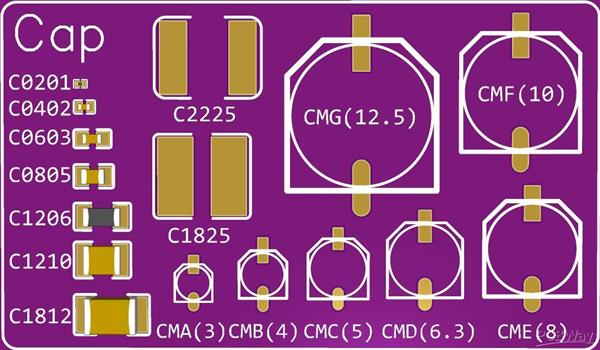
1. Screen-printed markings and their correspondences
The silkscreen layer on a PCB is primarily used to identify components, mounting holes, and alignment holes. To ensure a smooth PCB assembly process, all components, mounting holes, and alignment holes must have corresponding silkscreen markings. Generally, mounting holes on a PCB are labeled H1, H2, …, Hn to facilitate identification.
2. The principle of reading from left to right and from bottom to top
When designing screen-printed text, follow the principle of left-to-right and bottom-to-top. This helps improve the readability of the PCB. For polarized components, such as electrolytic capacitors and diodes, maintain consistent orientation within each functional unit to prevent installation errors.
3. Special Requirements for Pads and Solder Traces
To ensure the soldering reliability of components, there should generally be no silkscreen markings on the component pads. Similarly, there should be no silkscreen markings on the solder traces that require tin plating. This prevents the silkscreen markings from interfering with the soldering and tin plating processes, ensuring the continuity of the connection. In addition, component part numbers should not be obscured by installed components to facilitate insertion and repair. The spacing between silk-screen markings should generally be greater than 5 mil to ensure legibility.
4. Polarized Components and Directional Markings
For polarized components, the silkscreen should clearly indicate the polarity direction to facilitate identification by installers. Similarly, for connectors with a specified orientation, their orientation should also be clearly indicated on the silkscreen to prevent incorrect installation.
5. Barcode Location Markers
On the surface of the PCB, you may want to consider adding a 42×6 barcode screen-printed frame. This facilitates barcode scanning and provides a convenient way to track and identify the PCB.
6. Screen-printing information onto the finished board
PCBs should include silkscreen markings with manufacturing information, such as the board name, date, and version number. This information should be located on the PCB to facilitate easy identification and retrieval. This helps ensure the traceability and quality control of the PCB.
7. Manufacturer Information and Anti-Static Labels
PCBs should also include complete manufacturer information and anti-static labels. This information helps trace the origin of the PCBs and provides necessary safety and protection information.
8. Accuracy of Light Painting Files
The design and manufacture of PCBs require plot files. When preparing these files, it is essential to ensure that the number of layers is correct, that each layer is output correctly, and that all layers are included.
9. Consistency of Identifiers
The component identifiers on the PCB must match those in the BOM (Bill of Materials). This helps prevent confusion and incorrect installation.
Proper screen-printing layer design and implementation not only improve the readability of PCBs but also help reduce error rates during assembly and repair.
Frequently Asked Questions
1. What is the silkscreen layer on a PCB?
The silkscreen layer on a PCB consists of markings, patterns, and text printed on its surface. It is used to identify components, mounting holes, alignment holes, and other information to facilitate installation and repair.
2. Why is the "left-to-right, bottom-to-top" principle necessary?
This principle helps improve the legibility of PCB screen printing, making the information easier to recognize and understand.
3. Why is it necessary to avoid screen printing on device pads and solder traces?
Screen printing is avoided on device pads and solder traces to ensure the reliability of soldering and tinning, as screen printing may interfere with these processes.
4. What is a PCB BOM?
A BOM is the bill of materials for a PCB, which includes component identifiers and other key information used to guide the manufacturing process.
5. Why do PCBs need to be labeled with barcodes?
Barcode labels help track and identify PCBs, providing a means of monitoring production and quality control.
