

The warpage of a PCB refers to the flatness of its surface. If the PCB is not flat, it may not be positioned accurately, resulting in misalignment during component placement and potentially damaging the automated placement equipment.
In addition, printed circuit boards may warp after soldering, making it difficult to align component leads and to install them in enclosures or sockets.
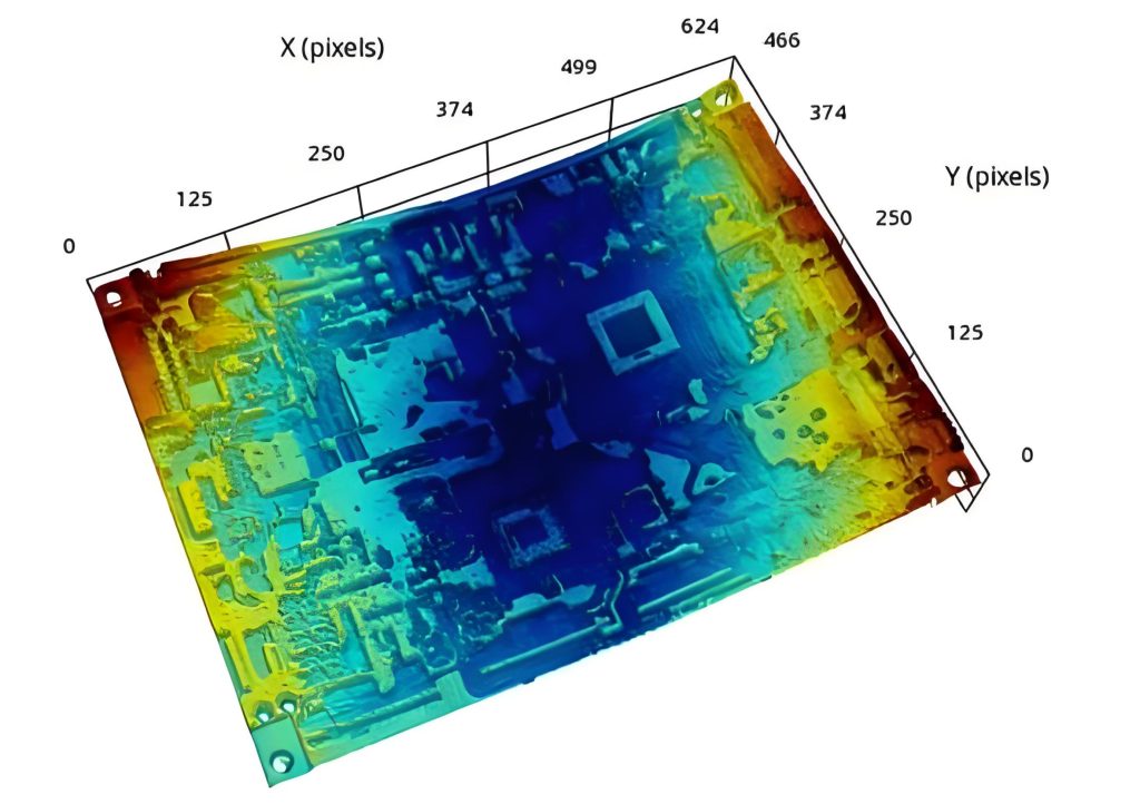
Standards for PCB Warpage
Standards for printed circuit board warpage are typically established in accordance with industry specifications. According to the U.S. IPC-6012 (1996 edition), the maximum allowable warpage and twist for surface-mount printed circuit boards is 0.75%, while other types of printed circuit boards are allowed a warpage of 1.5%.
This standard has raised the requirements for surface-mount printed circuit boards. In the field of high-reliability electronic products (such as military and aerospace equipment), the flatness requirements for PCBs are even more stringent, and the overall warpage limit may be reduced to 0.50% or lower.
How do you test the warpage of a printed circuit board?
Methods for testing the warpage of printed circuit boards typically follow international standards, such as GB 4677.5-84 or IPC-TM-650.2.4.22B.
During testing, place the circuit board on a calibrated platform, then insert a test probe at the point of greatest warpage. The warpage of the circuit board can be calculated based on the ratio of the test probe’s diameter to the length of the curved edge of the circuit board.
Formula for Calculating PCB Warpage
There are typically two methods for calculating PCB warpage:
① Method based on elevation difference:
Warp (%) = (H_{max} – H_{min}) / T × 100%
Among these:
H_{max}: The height of the highest point on the PCB surface above the horizontal plane
H_{min}: The height of the lowest point on the PCB surface above the horizontal plane
T: PCB Thickness
This method calculates warpage by measuring the height difference between the highest and lowest points on the PCB surface and comparing it to the board thickness.
② Methods based on length ratios:
Warpage (%) = (Height of Warp / Length of the Long Side of the PCB) × 100%
或
Warpage (%) = (Maximum single-corner warpage height / Substrate diagonal length) × 100%
The length of the diagonal can be calculated using the Pythagorean theorem.
The Relationship Between PCB Warpage and Automated Insertion Assembly
The warpage of a printed circuit board directly affects the efficiency and quality of automated insertion. The following are the key factors in this relationship:
- Component Placement Accuracy: If the circuit board warps, components may not be positioned accurately during insertion, which can lead to soldering issues and unstable performance of the electronic product.
- Damage to the insertion equipment: Unevenness in the circuit board may damage automatic insertion equipment, increasing the cost of repairs and equipment replacement.
- Welding Issues: Warping of the printed circuit board after soldering may cause component leads to become misaligned, thereby affecting soldering quality and reliability.
- Product Assembly: Bent circuit boards are difficult to install in enclosures or sockets and may require additional adjustments, which increases manufacturing costs and assembly time.
Frequently Asked Questions
Question 1: How does PCB warpage affect the performance of electronic products?
PCB warpage can affect the accuracy of component placement, potentially leading to soldering issues and unstable product performance.
Question 2: How can warpage in printed circuit boards be reduced?
To reduce warpage in printed circuit boards, you can select high-quality PCB materials, ensure proper temperature and pressure control during the manufacturing process, and make careful adjustments during product assembly.
