

With the continuous advancement of electronic technology, printed circuit boards (PCBs) have become a core component of modern electronic devices. To ensure the performance and reliability of PCBs, variousSurface TreatmentThese processes have been successfully applied. Among them, the tin-plating process—also known as Hot Air Solder Leveling (HASL)—plays a significant role in PCB manufacturing. This article will take an in-depth look at the working principles, process flow, and applications of the tin-plating process.
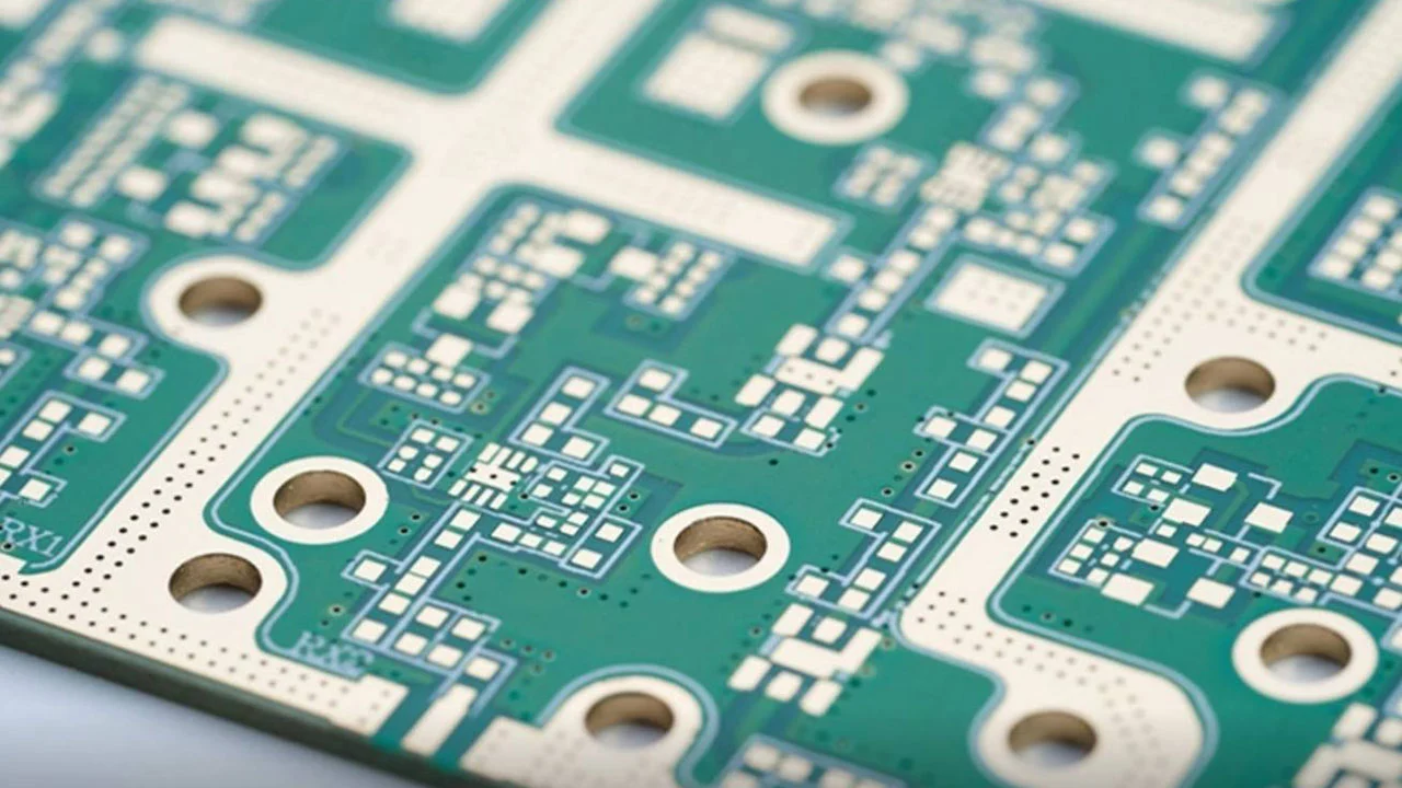
Table of Contents
- An Introduction to the Solder Spraying Process
- Process Flow and Its Functions
- Operational Procedures and Production Equipment
- Materials Used and Requirements
- Characteristics of the Tin-Spraying Process
- Frequently Asked Questions
- Conclusion
1. An Introduction to the Solder Spraying Process
The tin-spraying process, also known as hot-air leveling, is a surface treatment method commonly used in PCB manufacturing. The principle is simple: hot air is used to blow away excess molten tin from the surface of the PCB after it has been dipped in tin, thereby leveling the tin coating. This process ensures that the pads on the PCB surface have good solderability, guaranteeing that electronic components are reliably soldered to the PCB.
Advanced: The Relationship Between Solder Spraying and Lead-Free Manufacturing
The reason tin plating has endured for so long is that it fulfills three requirements simultaneously:Low cost, good solderability of the pads, and high tolerance for storage and multiple reflow cycles. To understand its place within the family of surface treatments, we must first clarify the differences between the leaded and lead-free approaches.
- Lead-containing HASL: Tin-lead alloys (typically Sn63/Pb37) have a melting point of approximately 183°C, excellent wettability, and a relatively smooth surface; due to RoHS restrictions, they are currently limited to exempt applications.
- Lead-Free HASL: The most common types are ternary alloys such as SnCuNi and SnCuCo, which have a melting point of approximately 227°C. Since the processing temperature is even higher, this places greater demands on both the heat resistance of the base material and the high-temperature resistance of the flux.
The ripple effects of the transition to lead-free soldering are worth noting: the tinning temperature has increased from approximately 250°C to 260–265°C. Although the board spends only a short time in the tin bath,Thermal shock has increased significantly...This is also one of the reasons why thin and large-size boards are more prone to warping after lead-free tin plating.
| Project | Lead-containing HASL | Lead-Free HASL |
|---|---|---|
| Common Alloys | Sn63/Pb37 | SnCuNi / SnCuCo |
| Melting Point | About 183°C | About 227°C |
| Tin Plating Temperature | About 250°C | 260–265°C |
| Wettability | 优 | Good (more dependent on flux) |
| Surface Flatness | Better | Slightly worse |
| Scope of Application | RoHS Exemptions | General-Purpose Lead-Free Products |
2. Process Flow and Its Functions
2.1 Micro-etching and Flux Treatment
Before tin plating a PCB, micro-etching and flux application are typically required. The primary purpose of these steps is to prepare the PCB for tin plating. Micro-etching prevents solder from failing to adhere or resulting in poor tin coverage, while the flux helps ensure uniform solder coverage.
2.2 Solder Spraying
During the tin-plating process, the PCB is immersed in molten solder and then quickly lifted out. A hot-air knife blows across the front and back of the board to level the liquid solder, ensuring an even layer on the copper surface and preventing solder bridges. This step is critical to the entire process, ensuring that the solder on the PCB surface is uniform and level.
2.3 Clean the tin surface and grinding plate with hot water
The purpose of cleaning the solder surface with hot water is to eliminate thermal expansion and contraction of the board caused by extreme temperature differences, while also removing residual flux, thereby improving solder joint quality. Board grinding further levels the solder surface to ensure its smoothness.
Advanced: Key Control Parameters for Vertical Hot-Air Leveling Machines
Fluctuations in tin plating quality are almost entirely attributable to equipment parameters rather than the process itself. The key control factors for vertical hot-air leveling machines can be summarized as “temperature first, airflow second, and time third”:
- Solder Pot Temperature: It is typically maintained at 30–45°C above the melting point. If the temperature is too high, it accelerates copper dissolution and the formation of tin dross; if it is too low, the molten tin has poor flow and cannot be spread evenly.
- Hot Air Knife Temperature and Pressure: The air knife temperature is generally close to the solder temperature; pressure determines the flattening effect; the air knife angle and distance from the board surface must be calibrated individually based on the board thickness.
- Tin Plating and Lift-Off Time: Excessively long tinning times can accelerate copper dissolution, while increasing the speed affects the amount of tin deposited and the risk of bridging.
- Preheating the Baking Sheet: If a board that hasn't been sufficiently preheated is placed directly into the solder, it will experience thermal shock, and thin boards are particularly prone to warping.
There are also two often-overlooked details on the device:Monitoring the Composition of Molten Tin(Excessive copper content can cause the tin layer to become brittle and reduce wettability) andTin Dross Cleanup Interval(Tin dross drawn into the air knife can cause scratches on the board surface.) If these two steps are carried out properly, the consistency between tin-plating batches will improve significantly.
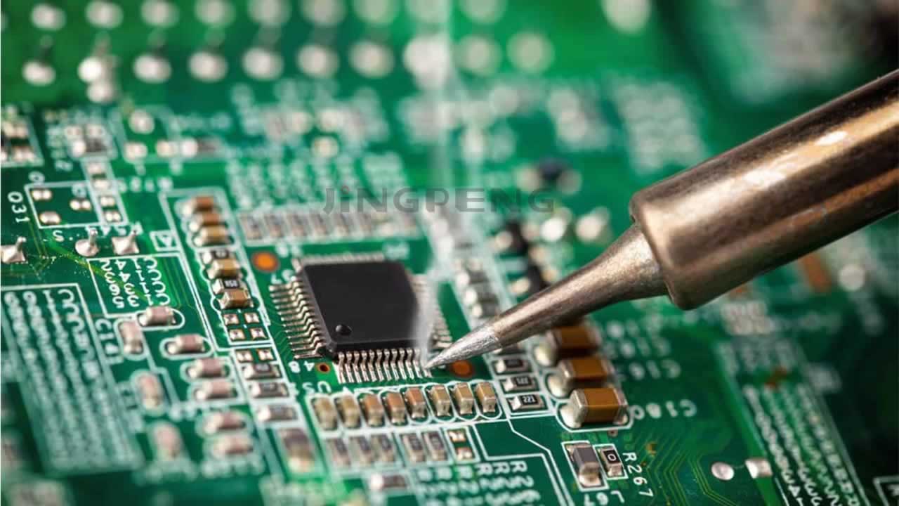
Solderability must ultimately be verified at the solder joint; solderability issues with tin-plated boards are typically related toSolderability of PCB HolesEvaluate the entire assembly, rather than just the appearance of the tin plating.
3. Operational Procedures and Production Equipment
The tin-spraying process typically requires specialized equipment known as vertical hot-air leveling machines. These machines feature precise temperature control and hot-air blades, which are used to evenly apply and level the solder on the PCB.
Advanced: How to Choose Lead-Free Solder Alloys
The differences among commonly used lead-free tin-plating alloys are primarily reflected in their melting points, wettability, and solder joint reliability:
| Alloy | Approximate melting point | Features | Common Uses |
|---|---|---|---|
| SnCuNi (SCN) | About 227°C | Low cost and moderate wettability; Ni can inhibit copper corrosion. | General-Purpose Lead-Free Solder Spray |
| SnCuCo | About 227°C | Co also inhibits corrosion, and the tin layer has a brighter appearance. | Products with specific appearance requirements |
| SnCuGe | About 227°C | Ge: Antioxidant; minimal tin dross formation | Extended periods of continuous production |
| SAC305 | About 217°C | Best wettability and reliability, but highest cost | High-reliability, fine-pitch applications |
When selecting an alloy, you can narrow down your choices based on the following criteria:
- Cost-sensitive and without fine-pitch components → SnCuNi is the most common default option;
- When there are requirements for the appearance of the tin-plated surface (e.g., exterior components of consumer products) → SnCuCo is preferred;
- Continuous production line operation and significant pressure regarding tin dross management → SnCuGe offers greater peace of mind;
- For applications with reliability certification requirements or fine-pitch BGAs → Confirm with the PCB manufacturer whether to switch to the SAC series or use an alternative surface treatment.
As for flux, the following is used for tin spraying:Specialized High-Temperature Flux...It must remain active at temperatures above 260°C and leave no residue after hot water cleaning. Insufficient flux activity directly results in poor tinning, while excessive activity increases the cleaning burden and may pose a risk of corrosion.
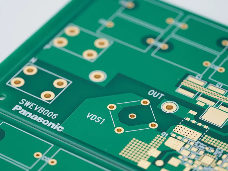
For a general comparison of surface treatments, please refer to4 Common PCB Surface Treatments... and tin plating is simply the lowest-cost option among them.
4. Materials Used and Requirements
In the tin-plating process, the solder typically used is lead-free solder, such as SnCuNi, SnCuCo, SnCuGe, or 305 solder. In addition, a high-temperature-resistant flux is required.
Advanced: The Quantitative Relationship Between Tin Thickness and Flatness
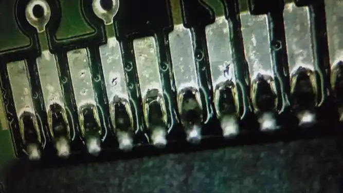
One of the most common criticisms of tin plating is thatUneven surface. After hot-air leveling, the thickness of the solder layer is uneven: it is thinner at the edges of the pads and thicker in the center, resulting in an overall slightly convex, arc-shaped profile.
- General Requirements for Solder Thickness on Pad Surfaces 2–5 μm, to ensure weldability;
- Typical Requirements for Hole-Internal Tin Thickness <25 μm(Some specifications allow for a maximum thickness of 38 μm); if the coating is too thick, it may cause pinholes or even clog the pores;
- Fine-pitch components (pitch ≤ 0.5 mm) are extremely sensitive to the flatness of the solder surface; uneven solder thickness directly affects placement alignment and soldering yield.
Therefore, there is a very practical criterion in engineering:When the minimum component pitch is greater than 0.65 mm and there are no high-density BGA packages, spray tin plating is usually sufficient; however, once the pitch reaches 0.5 mm or less, it is recommended to switch to flat surface finishes such as electroplated nickel-gold, electroless tin, or OSP.。
Precisely because of these flatness limitations, tin plating is generally not used forHDI (High-Density Interconnect) Board—Differences in the height of the solder surface between micro-pads make it difficult to consistently control solder paste printing and placement.
| Device Characteristics | Recommended Surface Treatments | Reason |
|---|---|---|
| Pitch ≥ 0.65 mm, no high-density BGA | Hot Air Solder Leveling (HASL) | Lowest cost, with sufficient weldability |
| 0.5 mm pitch or 0.5 mm BGA | OSP / Tin Plating | Smooth surface, manageable costs |
| BGAs of 0.4 mm or smaller that require multiple reflow cycles | ENIG (Electrolytic Nickel-in-Gold) | Smooth and long shelf life |
| Gold Fingers, Plug-in Wear Areas | Hard Gold Plating | Wear-resistant |
| Crimp Connectors | Tin Plating / Gold Plating | Crimp Hole Dimensions and Contact Reliability |
5. Characteristics of the Tin-Spraying Process
5.1 Tin Thickness Requirements
The solder pad surface on a PCB must meet certain tin thickness requirements. Generally, the tin thickness on the solder pad surface is approximately 2–5 micrometers, while the tin thickness inside the solder pad holes should be less than 25 micrometers (though this limit may sometimes be relaxed to 38 micrometers).
5.2 Scope of Application
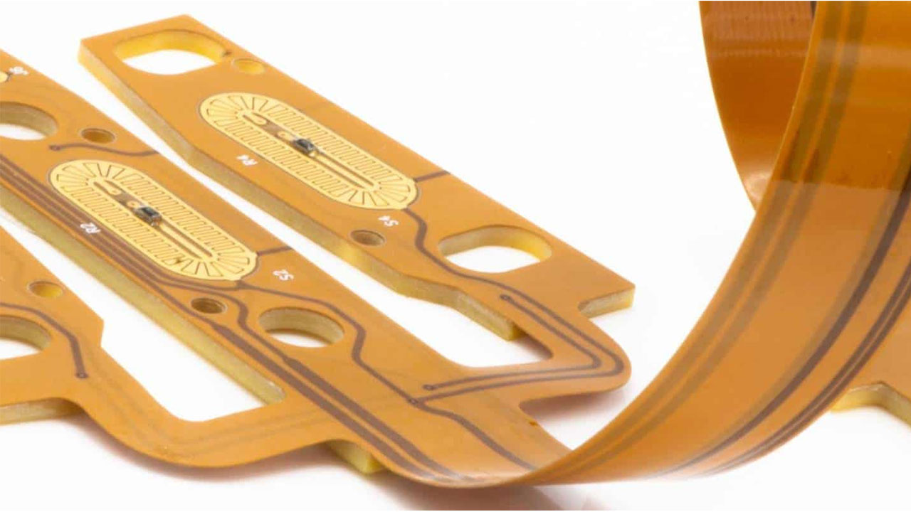
The coating produced by the tin-spraying process may not be sufficiently flat, so it is primarily suitable for PCBs with wide traces and large pads. However, this process is not typically used for high-density interconnect (HDI) boards.
5.3 Precautions
The tin-spraying process may produce an unpleasant odor during operation and is carried out at high temperatures, posing certain risks. Therefore, caution must be exercised when using this process, and relevant safety operating procedures must be followed.
Advanced: A Comparative Analysis of Solder Spraying and Other Surface Treatments
Comparing tin plating with several mainstream processes will make the selection process clearer:
| Process | Flatness | Solderability / Wettability | Storage Life | Cost | Typical Applications |
|---|---|---|---|---|---|
| HASL Solder Plating | 差 | 好 | 12 months or more | 低 | Wide-line, large pads; consumer electronics |
| Lead-Free HASL | Poor | 好 | Approximately 12 months | 低 | General-Purpose Lead-Free Products |
| ENIG (Electrolytic Nickel-in-Gold) | 优 | 好 | Approximately 12 months | Upper-middle | Fine-pitch BGAs, pushbuttons |
| OSP | 优 | Normal (decreases after multiple recirculations) | About 6 months | 低 | Large volumes, short lead times |
| Shen Xi | 优 | 好 | 6–12 months | 中 | Crimping, Fine Pitch |
| Hard Gold Plating | 优 | 好 | 长 | 高 | Gold fingers, plug-in wear zones |
Solder spraying also has another advantage that is often underestimated:Most tolerant of storage and multiple re-circulations. OSP coatings fail after repeated exposure to high temperatures, and electroplated gold carries the risk of “black pad,” whereas the tin layer applied by tin spraying will remelt when reheated and reform the solder joints, making it ideal for products that require multiple reworks or batch soldering over extended periods.
On the other hand, the shortcomings of tin plating are also clear: uneven surfaces, unsuitability for high-density boards, high heat resistance requirements for the boards due to high-temperature processes, and the presence of odors and heat-related risks in the operating environment. Therefore, it serves more as a “cost-effective fallback option” rather than the first choice for high-density designs.
If poor solder wetting has already occurred at the solder joint, you can refer toAnalysis of Causes and Solutions for PCB Soldering DefectsWhen troubleshooting step by step, the problem often lies not in the surface treatment itself.
Advanced: A Four-Step Inspection Process for Acceptance of Tin-Plated Sheets
Before conducting an incoming inspection or shipping, you can quickly go through the following four steps:
- Looking at the appearance: The tin coating should be continuous and shiny, with no exposed copper and no bridging; there should be no visible tin beads or sharp points at the edges of the pads.
- Measure the thickness of the tin: Use an X-ray thickness gauge to take random measurements of the pads and hole walls to verify that the pads are 2–5 μm thick and the hole walls are <25 μm thick.
- Solderability Testing: Conduct a wetting equilibrium test or a tinning test in accordance with the standard; the wetting time and wetting force must fall within the specified limits.
- Check for levelness: For boards with fine-pitch components, use coplanarity measurements to verify that the height variation of the solder surface is within acceptable limits.
It is important to note that,OSP Surface Treatment ProcessAlthough these alternatives offer better flatness, they are more sensitive to storage conditions and the number of welds; therefore, production line management requirements must be adjusted accordingly when changing processes.
6. Frequently Asked Questions
Q: How does the tin-spraying process differ from other surface treatment methods?
Answer: The tin-spraying process is a surface treatment method commonly used in PCB manufacturing. It works by using hot air to blow away excess molten tin, thereby leveling the tin surface. Compared to other methods, its advantages include ease of operation and suitability for PCBs with large pads and wide traces.
Q: How do I choose the right surface treatment method?
Answer: The choice of surface treatment method should be based on the specific PCB design and application requirements. The tin-spraying process is suitable for certain specific situations, but it is not suitable for all PCBs. Therefore, when selecting a surface treatment method, careful consideration must be given to the characteristics of the PCB and the required soldering performance.
Q: How many reflow soldering cycles can a tin-plated board withstand?
Answer: The solderability of the tin layer itself is well maintained; it can typically withstand 2–3 reflow cycles without a noticeable decrease in wettability, which is its advantage over OSP. However, it is important to note the heat resistance limits of the substrate and the device—the number of cycles is not unlimited.
Q: How long does it take for tin-plated sheet metal to deteriorate?
Answer: Under dry, room-temperature, vacuum, or moisture-proof packaging conditions, it generally remains stable for 12 monthsThat is all. If the storage environment is humid, the tin surface may oxidize and become dull. Before soldering, verify solderability; if necessary, use a mild-activating flux or desolder and repeat the process.
Q: Why is tin plating not recommended for HDI boards?
Answer: HDI boards feature small pad sizes and tight spacing; variations in the height of the tin layer resulting from spray tinning can cause uneven solder paste printing thickness and placement misalignment. Additionally, it is difficult to completely blow away residual tin from the microvias, so the risks outweigh the benefits.
Q: Can tin plating and electroless gold plating be used together on the same board?
Answer: Selective surface treatment (such as localized gold plating combined with overall tin plating) is possible, but the process is complex, costs are higher, and plating bleed and contamination are likely to occur at the interface. This option should only be considered when it is truly necessary to balance cost with the requirement for fine pitch in specific areas.
Q: Will uneven tin thickness affect surface-mount assembly?
Answer: Yes. Differences in the solder surface height can cause inconsistent solder paste print thickness, which can lead to bridging or solder deficiency in fine-pitch components. During placement, inconsistent support heights can also cause misalignment.
Q: Why is lead-free solder spraying more likely to cause thin sheets to warp?
A: Because the tin-plating temperature rises from approximately 250°C to 260–265°C, the thermal shock is more severe; thin sheets lack sufficient rigidity, so thermal contraction after exiting the furnace is more likely to cause warping. This can be mitigated by increasing the preheating time, using support fixtures, and reducing the cooling rate.
Q: Why do tin beads remain in the holes of tin-plated boards?
A: This is primarily caused by the hot air knife failing to completely blow the molten solder out of the via, or by a via diameter-to-board-thickness ratio that is too high, resulting in solder buildup. Minor cases can be resolved in subsequent processes, but severe cases can cause the via diameter to exceed tolerance limits or even lead to via blockage, requiring adjustments to the air knife pressure and lifting speed parameters.
Q: How can you quickly assess the quality of a tin plating layer?
Answer: Three steps: First, check whether the tin surface is continuous and shiny, with no exposed copper or bridging; next, randomly sample the solder pad and via to verify that the tin thickness falls within specifications; finally, perform a wetting equilibrium or tinning test to confirm solderability. The component is considered合格 only if all three steps are passed.
Q: Is tin-plated board suitable for making gold fingers?
Answer: No, it is not suitable. Gold fingers require a hard, wear-resistant gold plating layer; the tin coating applied by spray plating has low hardness and is prone to wear and oxidation, which will reduce contact reliability after just a few insertions and removals.
7. Conclusion
The tin-plating process is one of the most commonly used surface treatment methods in PCB manufacturing. It ensures uniform coating and leveling of the pad surfaces, thereby improving soldering quality. However, it is not suitable for all PCBs, so when selecting a surface treatment method, it is necessary to evaluate the options based on specific requirements. If you would like more information about PCB manufacturing or surface treatment, please feel free to contact us.
Related Recommendations:How to Choose a PCB Surface Treatment Process · Advantages and Disadvantages of Seven Common Surface Treatment Processes for PCBs
