

Want to learn about the various methods of PCB surface treatment and their pros and cons? This blog will introduce you to different PCB surface treatment technologies and help you understand the advantages and limitations of each method. We’ll delve into the benefits and potential challenges of each technology, enabling you to choose the most suitable treatment solution based on your project’s requirements. Optimize your PCB design and manufacturing processes to enhance the performance and stability of your electronic products.
There are many types of surface treatments for circuit boards, and PCB prototyping professionals must select the appropriate one based on the board’s performance and requirements. Below is a brief analysis of the advantages and disadvantages of seven common PCB surface treatments for your reference!
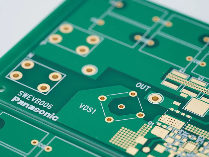
HASL Hot-Air Leveling (Tin Plating)
Tin plating was a common process used in the early days of PCB manufacturing. Today, it is divided into leaded and lead-free tin plating.
What Is Tin Plating?
Tin plating is a common surface treatment method used in electronics manufacturing. It involves spraying molten tin alloy onto the surface of a PCB (Printed Circuit Board) to form a thin layer of tin. The purpose of this process is to improve the solderability of the PCB surface and enhance the reliability of soldered connections.
In the PCB assembly process, tin plating is primarily used to coat the pads and pins on the PCB surface. When assembling components (such as electronic components), the pads and pins are heated so that they melt and fuse with the tin coating, forming a reliable solder joint. The advantages of tin plating include fast soldering speeds, consistent soldering quality, and the ability to prevent oxidation of the pads. This makes tin plating a commonly used surface treatment technique, particularly well-suited for large-scale, automated production environments.
Advantages of Solder Spray
- Longer storage time
- After the PCB was completed, the copper surface was fully wetted (completely covered with solder before soldering).
- Suitable for lead-free soldering
- Proven technology
- Low cost
- Suitable for visual inspection and electrical testing
The Weaknesses of Solder Spray
- Not suitable for wire bonding; due to surface flatness issues, it also has limitations in SMT; not suitable for contact switch designs.
- During tin plating, the copper dissolves, and the board is exposed to high temperatures.
- For particularly thick or thin sheets, tin plating has its limitations, and the production process is cumbersome.
OSP (Organic Protective Layer)
What is OSP?
OSP is one of the common surface treatment technologies used in PCB manufacturing. Its full English name is ”Organic Solderability Preservatives,” and it is known in Chinese as ”organic solderability preservatives.” OSP is primarily used to protect the surface of PCBs from oxidation in the air, while also providing good solderability.
During the OSP surface treatment process, a layer of organic solderability preservative is applied to the surface of the PCB. This thin protective layer effectively shields the PCB pads and pins from oxidation and corrosion. Since this protective layer is composed of organic materials, it evaporates at high temperatures, allowing for good contact with the solder during the soldering process and facilitating the soldering operation.
【Click here to learn more about OSP】
Advantages of OSP
- The manufacturing process is simple, and the surface is very smooth, making it suitable for lead-free soldering and SMT.
- It is easy to rework, simple to operate, and suitable for horizontal line operations.
- The board is suitable for multiple surface treatments to be applied simultaneously (e.g., OSP + ENIG).
- Low cost and environmentally friendly.
Weaknesses of OSP
- Limit on the Number of Reflow Soldering Cycles (Repeated soldering on thick films can damage the film; generally, two cycles are fine)
- Not suitable for crimping; use wire binding instead.
- Visual and electrical inspections are inconvenient.
- N2 gas protection is required during SMT.
- SMT rework is not suitable.
- Storage conditions are demanding.
Chemical silver
What Is Chemical Silver?
Chemical silver plating is a common surface treatment technique used in electronic manufacturing. It involves applying a layer of silver chemical solution to the surface of a PCB (Printed Circuit Board) to form a thin layer of silver. The purpose of this process is to improve the electrical conductivity and solderability of the PCB surface, thereby enhancing the reliability of soldered connections.
In the chemical silver plating process, the chemicals used are typically solutions containing silver ions. These solutions react with the PCB surface, reducing the silver ions to solid, pure silver. This creates a dense, smooth silver layer that gives the PCB surface good electrical conductivity and excellent solderability.
Advantages of Chemical Silver
- The manufacturing process is simple and suitable for lead-free soldering and SMT.
- The surface is very smooth
- Suitable for very fine lines.
- Low cost.
The Weaknesses of Chemical Silver
- It has strict storage requirements and is prone to contamination.
- Weld strength is prone to problems (micro-porosity).
- Electromigration is likely to occur, as is Galvanic corrosion of the copper beneath the solder mask.
- Electrical testing is also an issue.
Chemical Tin
What Is Chemical Tin?
Chemical tin plating involves applying a layer of tin-based chemical solution to the surface of a PCB (Printed Circuit Board) to form a thin layer of tin. The purpose of this process is to improve the solderability of the PCB surface and enhance the reliability of soldered joints.
In the chemical tin plating process, the chemicals used are typically solutions containing tin ions. This solution undergoes a chemical reaction on the surface of the PCB, reducing the tin ions to solid tin. This forms a uniform and dense tin layer, giving the PCB surface good solderability and excellent corrosion resistance.
In chemistry, tin is the most reactive metal in copper-tin displacement reactions.
Advantages of Chemical Tin
- Suitable for horizontal production lines.
- Suitable for fine-line processing, lead-free soldering, and especially crimping.
- Excellent flatness, suitable for SMT.
The Weaknesses of Chemical Tin
- Proper storage conditions are required; it is best not to store the product for more than 6 months to control tin whisker growth.
- Not suitable for contact switch designs
- The production process places high demands on the solder mask application process; otherwise, the solder mask may peel off.
- For multiple welds, it is best to use N2 gas shielding.
- Electrical testing is also an issue.
Electrolytic Nickel-Gold (ENIG)
What Is Chemical Nickel-Gold?
Chemical nickel-gold plating involves applying a layer of nickel-gold chemical solution to the surface of a PCB (Printed Circuit Board) to form a thin layer of nickel-gold. The purpose of this process is to improve the PCB’s surface conductivity, corrosion resistance, and solderability, thereby enhancing the reliability of soldered connections.
In the chemical nickel-gold plating process, a layer of nickel is first deposited onto the surface of the PCB, followed by a layer of gold on top of the nickel layer. This is achieved using a chemical solution containing nickel ions and gold ions. The thickness of the electroless nickel-gold layer can be adjusted as needed and is typically controlled within a range of a few micrometers.
Advantages of Nickel-Gold Plating
- Suitable for lead-free soldering.
- The surface is very smooth, making it suitable for SMT.
- Through-holes can also be plated with nickel-gold.
- Longer storage life; storage conditions are not stringent.
- Suitable for electrical testing.
- Suitable for switch contact design.
- Suitable for binding aluminum wire and thick plates; highly resistant to environmental corrosion.
Disadvantages of Electrolytic Nickel-Gold Plating
- Higher costs
- The process is complex
- Environmental Impact
- Limited coating thickness
- Sensitive to extreme environmental conditions
Electroplated Nickel-Gold
What Is Nickel-Gold Plating?
Electroplating nickel-gold involves using an electrochemical reaction to form a layer of nickel-gold on the surface of a metal. The purpose of this process is to improve the metal’s surface hardness, corrosion resistance, and aesthetic appeal.
Electroplating nickel-gold typically involves immersing a metal surface in an electrolyte containing nickel ions and applying an electric current to reduce the nickel ions into a solid nickel-gold layer. This nickel-gold layer adheres uniformly to the metal surface, forming a dense and smooth protective coating.
Electroplated nickel-gold is divided into “hard gold” and “soft gold.” Hard gold (such as gold-cobalt alloys) is commonly used on gold fingers (in contact connection designs), while soft gold refers to pure gold. Nickel-gold plating is widely used on IC carrier boards (such as PBGA), primarily for bonding gold and copper wires. However, for IC carrier boards, the plating process requires additional conductive lines to be created in the gold-finger bonding area before plating can be applied.
Advantages of Nickel-Gold Plating
- Longer storage period > 12 months.
- Suitable for contact switch design and gold wire bonding.
- Suitable for electrical testing
Weaknesses of Nickel-Gold Plating
- Higher cost; the gold layer is thicker.
- When electroplating gold fingers, additional conductive traces are required in the design.
- Because the thickness of the gold varies, when used in soldering, the solder joints may become brittle due to excessive gold thickness, which can compromise their strength.
- Issues with the uniformity of the electroplated surface.
- The nickel-gold plating does not cover the edges of the wire.
- Not suitable for binding with aluminum wire.
Nickel-Palladium-Gold (ENEPIG)
What Is Nickel-Palladium-Gold?
Nickel-palladium plating is a common surface treatment technique, also known as nickel-palladium alloy plating. It involves depositing an alloy of nickel and palladium onto a metal surface through an electrochemical reaction, thereby forming a layer of nickel-palladium metal. The purpose of this process is to improve the metal surface’s corrosion resistance, hardness, and aesthetic appeal.
Nickel-palladium electroplating typically involves immersing a metal surface in an electrolyte containing nickel and palladium ions, and applying an electric current to reduce the nickel and palladium ions into a solid layer of nickel-palladium alloy. This nickel-palladium metal layer adheres uniformly to the metal surface, forming a dense and smooth protective layer.
Advantages of Nickel-Palladium-Gold
- For use on IC carrier boards; suitable for gold wire bonding and aluminum wire bonding. Suitable for lead-free soldering.
- Compared to ENIG, it does not have the problem of nickel corrosion (black plating); it is less expensive than ENIG and electroless nickel-gold plating.
- Long storage life.
- Suitable for a variety of surface treatment processes and present on the board.
The Weaknesses of Nickel-Palladium-Gold
- The process is complex and difficult to control.
- It has a short history of application in the PCB industry.
The above outlines the advantages and disadvantages of seven common surface treatment processes for PCBs. If you still have questions about surface treatment for your new project, please feel free to contact the engineers at Jingpeng Electronics. We will provide you with sound recommendations for your project. 0755-23214901
