

After the PCB has undergoneReflow SolderingDuring the manufacturing process, issues such as board warping and bending often arise, and in some cases, these can even lead to cold solder joints or component tombstoning—problems that cause significant headaches for the electronics manufacturing industry. Therefore, we need to gain a thorough understanding of the causes of these issues and how to take measures to overcome them.
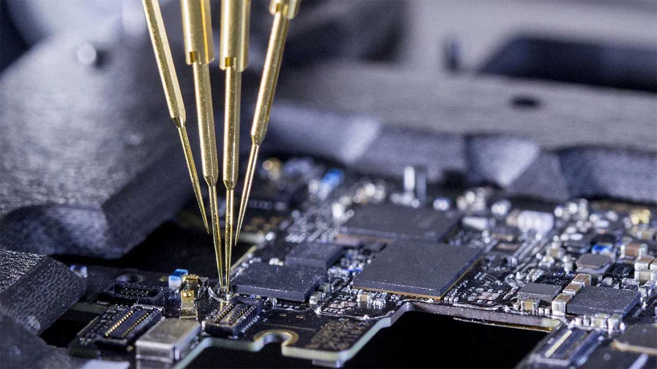
1. The Dangers of PCB Warping
On an automated surface-mount assembly line, an uneven circuit board can cause the following problems:
1.1. Inaccurate positioning
An uneven circuit board can prevent components from being positioned accurately in their designated locations, which may affect the overall performance of the circuit.
1.2. Insertion Issues
Components may not fit into the holes or surface-mount pads on the board, which can hinder the proper assembly of the circuit.
1.3. Damage to the Automatic Insertion Machine
If a circuit board with components mounted on it warps after soldering, it may cause damage to the automatic insertion machine, thereby increasing maintenance and repair costs.
1.4. Part Cutting Issues
Warping of the circuit board can also make it difficult to trim component leads straight and even, which may lead to soldering issues and reduced performance.
1.5. Chassis Assembly Issues
A warped circuit board may not fit into the chassis or the sockets inside the device, which could affect the assembly of the entire product.
To address these issues, current surface-mount technology is constantly evolving, requiring higher levels of flatness in printed circuit boards.
IPC standards specifically state that the maximum allowable warpage for PCBs with surface-mount components is 0.75%, while the maximum allowable warpage for PCBs without surface-mount components is 1.5%. In practice, to meet the demands of high-precision and high-speed assembly, some electronics assembly manufacturers have even stricter requirements for warpage. For example, some customers require a maximum allowable warpage of 0.5%, and a few even specify 0.3%. This further highlights the critical importance of PCB flatness.
Printed circuit boards (PCBs) are composed of various materials, including copper foil, resin, and glass cloth. These materials have different physical and chemical properties, and they interact with one another during processing and manufacturing, generating residual thermal stress that can cause the PCB to warp. In addition, during the PCB manufacturing process, the boards undergo various procedures—such as exposure to high temperatures, mechanical cutting, and wet processing—which also significantly contribute to board warpage. In summary, the causes of PCB warpage are complex and diverse.
Advanced: First, distinguish between the three forms of deformation
Before identifying the cause, let’s first break down the concept of “deformation” itself. In engineering, deformations are typically classified into three categories based on their shape, and the methods for determining them and the approaches to correcting them differ accordingly:
- Bow: The board surface is generally curved in a cylindrical or spherical shape, with the four corners still largely lying in the same plane. This is often caused by asymmetrical layering and uneven copper distribution; corrective measures should focus on the layering and copper plating processes.
- Twist: The four corners are not in the same plane and are raised diagonally. This is often related to differences between the material’s warp and weft directions, residual stress from pressing, and the orientation of the V-cut.
- Corner Curling and Localized Curling: Warping in a specific corner or area is typically related to large copper areas, heavy components, or panel-splitting stress.
The reason for making this distinction is thatThe causes of warping and twisting are different; adjusting the reflow soldering profile can only resolve some of these issues.. If the diagnosis is incorrect, the subsequent corrective actions are often in vain.
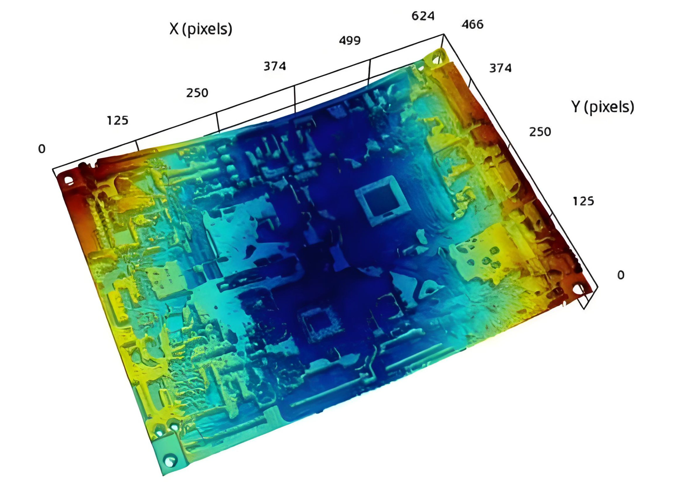
For a more systematic classification and testing method, please refer toAn In-Depth Understanding of Warpage in PCBs and PCBA。
2. Analysis of the Causes of PCB Warpage
To address the issue of PCB warping, we need to conduct an in-depth analysis of its causes, which primarily include the following aspects:
2.1. Uneven copper plating on the circuit board
Typically, circuit boards are designed with large areas of copper foil to serve as ground planes; sometimes, the Vcc layer is also designed with large areas of copper foil. However, if these large areas of copper foil are not evenly distributed across the same circuit board, it can lead to uneven heat absorption and dissipation. As the circuit board expands and contracts with temperature changes, inconsistent expansion and contraction may generate stress, causing the board to deform.
2.2. The connection points (vias) between the layers of a circuit board can restrict the board's expansion and contraction.
Most circuit boards today are multilayer boards, and there are connection points (vias) between the layers. These connection points are classified as through-holes, blind vias, and buried vias. These connection points restrict the board’s ability to expand and contract, which can indirectly cause the board to bend or warp.
2.3. Weight of the Circuit Board
The weight of the circuit board itself can cause it to sag and deform. Reflow ovens typically use a chain to move the circuit board through the oven, with the board’s edges serving as fulcrums. If the board has components that are too heavy or if the board is too large, its own weight can cause the center to sag, resulting in board warpage.
2.4. V-Cut Depth and Connecting Strips
V-Cut is the main cause of structural damage to the board. Because V-Cut involves cutting grooves into a single large sheet of material, the areas where V-Cut is applied are prone to deformation.
2.5. The Effect of Laminated Materials, Structures, and Patterns on Panel Deformation
A PCB is formed by laminating a core board, prepreg, and outer copper foil. Since prepreg naturally expands and contracts with temperature changes, the core board and copper foil have different coefficients of thermal expansion. Consequently, warping often occurs in PCBs. This issue can be mitigated during the PCB design phase by controlling the areas where the outer copper foil is laid.
Advanced: Quantitative Control of Material and Laminate Symmetry
The root cause of the distortion isStress is distributed unevenly within the plate... Stress primarily arises from three sources: the material’s own thermal expansion, residual stress left over from the pressing process, and repeated thermal cycles during processing and welding. From a design perspective, the first of these is the primary factor that can be controlled.
- Layer Symmetry: The thickness of the dielectric, the copper, and the arrangement of the core layers must all be symmetrical about the center of the board; if any one side is thicker, it will pull the board to that side.
- Copper is evenly distributed: When laying out a large copper area, ensure that the copper surface corresponds to the symmetrical layer; it is recommended to fill in any blank areas.Balance Copper (dummy / thieving copper), rather than leaving it blank.
- Material Matching: The resin system and glass cloth grade of the core board and the prepreg should be consistent; the greater the difference in CTE, the greater the internal stress after lamination.
- Plate Thickness to Dimension Ratio: Thin, large panels are most prone to warping; if necessary, increase the panel thickness or add support points.
| Verification Items | Requirements | Consequences of Common Deviations |
|---|---|---|
| Core Panel Layout | About Central Symmetry | Uneven number of layers or thickness → Unidirectional warping |
| Media Thickness | Symmetrical top and bottom, same model | Blending Different PP Types → Differences in CTE |
| Copper Thickness | Symmetry Across All Levels | Inconsistent outer copper layer thickness → Warping |
| Scrap Copper Rate | The levels are close together; we recommend ≥60%. | Excessive difference → Deflection after compression |
| Glass Cloth Models | Same floor, same model | Mixing 1080 and 2116 can cause warping |
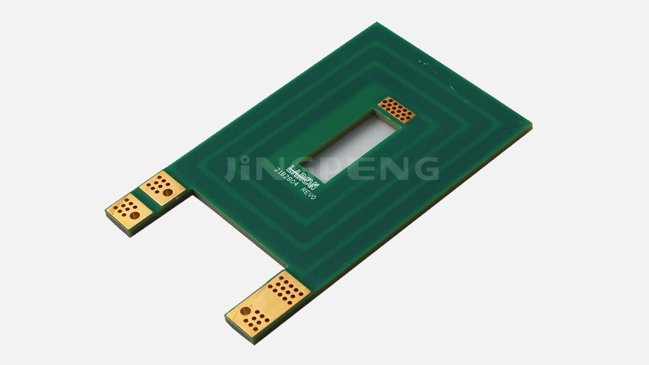
Details on pairing prepregs with core panels can be found inAn Introduction to Multilayer Board Substrate Materials and Pre-pregsThere are more detailed instructions there; issues related to symmetry should be resolved during the material selection phase.
3. Solutions for PCB Warping
To address the causes of warping mentioned above, we can take the following measures to resolve PCB warping issues:
3.1. Selection of Materials
Select substrate materials with a low coefficient of thermal expansion to minimize warping and buckling caused by thermal stress. Additionally, ensure the uniformity and quality of the materials.
3.2. Design Considerations
During the PCB design phase, it is important to plan the distribution of copper foil appropriately to avoid uneven copper layup and reduce thermal stress. The board thickness should be designed appropriately, and the V-cut depth and location of the connecting bars should be selected carefully.
3.3. Process Control
Control the temperature profile of the reflow soldering process to avoid excessive temperature gradients. Use support fixtures during the soldering process to prevent board warping. Apply appropriate reflow soldering process parameters to ensure uniform soldering.
Advanced: How to Match Reflow Soldering Curves with Support Fixtures
Even if the design is sound, the reflow process itself can cause warpage. Warpage in circuit boards during soldering is primarily caused by three factors:
- Temperature Gradient: The greater the temperature difference across the surface of the plate—both vertically and horizontally—the more out of sync the thermal expansion and contraction will be. Reducing the heating rate and extending the temperature equalization time are the most direct ways to mitigate this issue.
- Sagging Due to Body Weight: When a chain or mesh belt is supported at both ends of a panel and suspended in the middle, the center will sag if the panel is large or the components are heavy. The solution is toAdd support fixtures or switch to using pallets。
- Cooling Rate: If the plate cools too quickly after coming out of the furnace, the stress is trapped inside the plate before it has a chance to release; slowing down the cooling process appropriately helps the plate return to a flat state.
| Stage | Frequently Asked Questions | Adjust Direction |
|---|---|---|
| Warming Zone | Excessively high speed, large temperature differences across the board | Decrease to 1.5–2.5 °C/s |
| Tempering Zone | Insufficient time, insufficient flux activation | Extended to 60–120 seconds |
| Backflow Zone | Peak values are too high and exceed the material's heat resistance | Minimize the peak value as much as possible while maintaining solderability |
| Cooling Zone | Excessively rapid cooling, stress locking | Slow down to 3–6 °C/s |

For system practices on the production line side, please refer to the following:6 Steps to Prevent PCB Warpage...It separates design operations from production line operations, making it easier to compare and implement them.
3.4. Sheet Metal Fabrication
During the cutting and processing of sheet metal, care must be taken to avoid mechanical damage and excessive stress. Select the appropriate V-Cut process and control the cutting depth to minimize damage to the sheet metal.
3.5. Quality Control
Establish a comprehensive quality control system, including inspection and testing of circuit boards, to promptly identify and address deformation issues.
3.6. Special Handling
For applications that require extremely high flatness of the sheet material, special treatment methods—such as hot-press flattening—may be considered.
Advanced: How Exactly to Measure and Evaluate Warpage
A standardized measurement method is essential for determining whether a value exceeds the limit; otherwise, it is easy for people to interpret the results differently. The industry-standard practice is IPC-TM-650 2.4.22:
- Place the board on the standard platform so that the three lowest points among its four corners touch the platform;
- Measure the maximum gap D between the fourth corner and the platform;
- Measure the length L of the board's diagonal;
- Warp = D ÷ L × 100%.
The determination threshold is generally:Boards with surface-mount components are allowed 0.75%, while boards without surface-mount components are allowed 1.5%.; Customers with high-precision placement requirements often adjust the tension themselves to 0.51 TP3T, and some even require 0.31 TP3T.
| Panel Type | General Requirements | Strictly Adhere to Common Customer Requirements |
|---|---|---|
| Board with SMD components | 0.75% | 0.5% / 0.3% |
| Board without SMDs | 1.5% | 1.0% |
| Large-Size Backplates / Thick Plates | Under the Supply and Demand Agreement | Under the Supply and Demand Agreement |
For complete test procedures and evaluation criteria, seeStandards and Test Methods for PCB Warpage。
Advanced: Six-Step Procedure for Handling Excessive Deformation
Once you discover that a value exceeds the limit, troubleshooting in the following order is the most efficient way to proceed and will help you avoid repeated trial and error:
- First, let's standardize the measurement conditions.: The mounting method, duration of exposure, and ambient temperature can all affect the readings; verify that the readings actually exceed the threshold;
- Check for Layers and Residual Copper Content: First, check whether the design is symmetrical; this step involves the lowest cost and yields the greatest benefit;
- Verify the lamination parameters and the sheet batch: Exclude material variations and issues with the pressing process;
- Adjust the Reflow Soldering Profile: Reduce the heating rate, extend the temperature equalization period, and slow down the cooling rate;
- Add support fixtures or pallets: Reduce sagging caused by the component's own weight during reflow;
- Consider hot-press flattening only as a last resort: It can push the plate back into place, but the stress has not been eliminated, so the deformation may reoccur during subsequent flow.
In other words, hot-press leveling is a type ofCorrective Action...The truly reliable approach is to go back to Steps 2 and 3 and balance the design with the stresses in the material.
Advanced: Six Requirements to Include in the Design Specifications Before Submitting the Proposal
Rather than waiting for problems to arise before making corrections, it’s better to clearly specify the requirements at the PCB design stage. The following six recommendations should be explicitly noted in the drawings or specifications:
- Define the Warpage Threshold: Please specify whether it is 0.75% or 0.5%; do not just write “per IPC”;
- Lamination Requirements: Symmetry, consistent dielectric type, and symmetrical copper thickness;
- Residual Copper Content Requirements: Balanced across all layers, allowing PCB manufacturers to add balancing copper in blank areas;
- Support and Weight Information: Specify the board's mounting method, maximum component weight, and dimensions to facilitate the board manufacturer's evaluation of the production fixtures;
- V-Cut and Spacer Bar Position: Avoid placing heavy and precision components to prevent stress from the panel-separation process from being transferred to the board;
- Special Area Markings: Specify separately for areas sensitive to flatness, such as those beneath the BGA.
The panel layout also affects panel separation stress; for comparison, seePCB Panelization MethodsChoose the most appropriate connection type.
In summary, the issue of PCB warpage is a multifaceted problem that must be addressed from multiple angles, including material selection, design, process control, manufacturing, and quality control. Only by comprehensively considering these factors can PCB warpage be effectively minimized or prevented, thereby ensuring the quality and reliability of electronic products. Therefore, electronics manufacturers should pay close attention to these details and continuously improve their manufacturing capabilities to meet market demand for high-quality electronic products.
Related Reading:An Introduction to Multilayer Board Substrate Materials and Pre-pregs · Causes and Solutions for Open Circuits in PCBs
4. Frequently Asked Questions
Q: How exactly should we interpret IPC's 0.75% and 1.5%?
Answer: It is the upper limit for warpage (maximum gap ÷ diagonal length): 0.75% for boards with surface-mount components, and 1.5% for those without. This is merely a general industry threshold; specific projects may set stricter standards based on mounting accuracy.
Q: Which is more serious, a curvature or a twist?
A: You can’t simply compare the severity; it depends on the context. Warping causes both diagonals to lose coplanarity simultaneously, which has a more direct impact on fine-pitch devices; buckling is typically more pronounced but has a regular shape, making it easier to flatten using fixtures. The key to determining the appropriate course of action is to first identify the specific type of deformation before discussing corrective measures.
Q: Does adding balancing copper affect electrical performance?
A: Generally not, because it is an unconnected isolated copper area that does not participate in signal return paths. However, care must be taken to maintain adequate spacing from high-speed signal lines to avoid introducing additional coupling into sensitive lines; if necessary, have the PCB manufacturer route the traces around them according to the rules.
Q: Are thin sheets necessarily more prone to warping?
Answer: Generally speaking, yes. The thinner the board, the lower its rigidity; the same stress will cause greater deformation. Therefore, boards thinner than 0.6 mm require special attention to layer symmetry and oven support.
Q: What is the appropriate depth for a V-cut?
Answer: Typically, one-third of the board thickness is retained as the connection thickness (i.e., the cutting depth is approximately two-thirds), though this depends on the board thickness and the method of separation. Cutting too deeply can cause deformation before separation, while cutting too shallowly makes separation difficult and leads to stress concentration.
Q: Is it safe to use the panels after they’ve been heat-pressed and flattened?
Answer: It can be used as a corrective measure, but keep in mind that it merely presses the board back into shape; the internal stress has not been released. If the board is to undergo reflow soldering afterward, warpage may recur; therefore, we recommend conducting validation tests for critical batches.
Q: Can board warping cause BGA solder joint defects?
Answer: Yes. When the board surface is uneven, the contact height between the BGA solder balls and the solder paste is inconsistent, making the edge balls prone to open circuits or bridging. This can result in localized cold solder joints after reflow, which is also one of the key factors in controlling warpage.
Q: Why do some boards in the same batch warp while others do not?
A: This is typically related to the lamination layout, material batch, storage conditions, and whether the component has undergone reflow. We recommend first compiling statistics by batch and location. If a pattern emerges (such as in a specific area), it is most likely due to a lamination or layering issue; if the defects are scattered, it is more likely due to moisture absorption during storage or fluctuations in reflow conditions.
Q: Can deformation and open-circuit problems occur at the same time?
Answer: Yes. Severe warping can subject the via walls and solder joints to additional stress, which may lead to via copper cracks or solder joint fractures, manifesting as intermittent open circuits. For more information, please refer toCauses and Solutions for Open Circuits in PCBsConduct a cross-check.
