

In the production and application of printed circuit boards (PCBs), pad oxidation has always been a key challenge affecting product yield.
Unprotected bare copper pads exposed to the air can develop an oxide layer in as little as 4 hours. This oxide layer directly prevents solder from effectively wetting the copper surface during subsequent soldering, significantly increasing the rate of cold solder joints—by 30% or more—and, in severe cases, can even result in the entire batch of PCBs being scrapped.
The OSP (Organic Solderable Protective Layer) process, as the mainstream technology for addressing this issue, has been widely adopted in the consumer electronics and home appliance industries due to its low cost and high planeness.
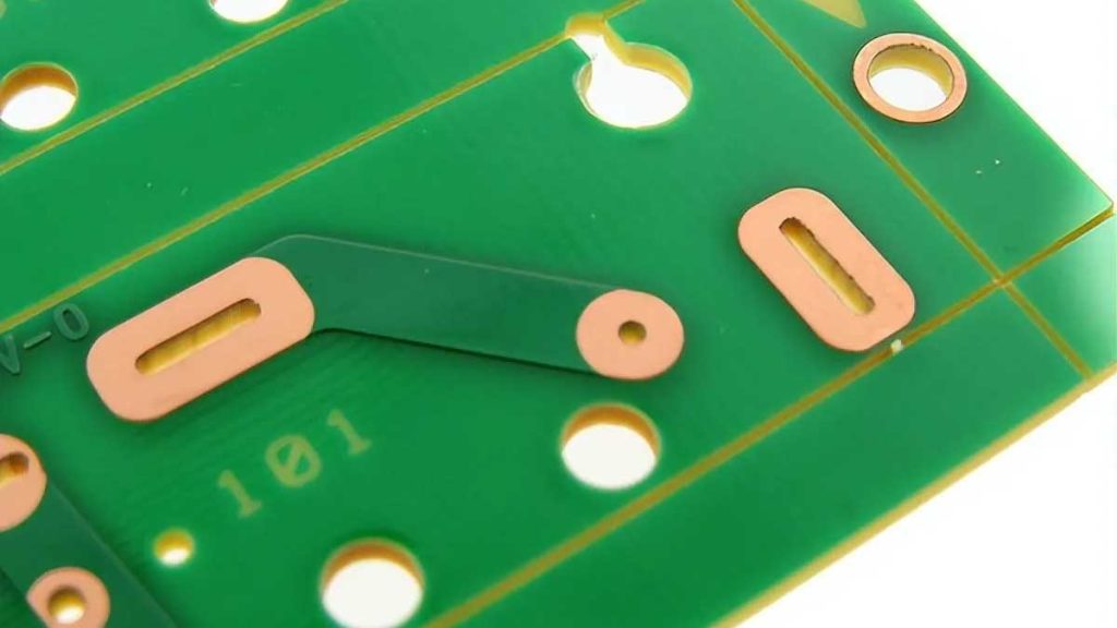
So, what exactly is the OSP process?
How does its operating principle ensure the solderability of the pads?
Compared to other surface treatment processes, such as gold plating and tin plating, what are its unique advantages and limitations?
This article provides a comprehensive breakdown of the OSP process—from basic definitions to practical applications—to offer PCB design and manufacturing professionals a clear technical reference, helping them accurately determine whether the OSP process is suitable for their projects.
Basic Understanding of the OSP Process: Definition and Key Functions
What is the OSP process?
The OSP process, which stands for Organic Solderability Preservative, is a surface treatment technology that uses chemical deposition to form an ultra-thin organic protective film on the bare copper surface of a PCB.
The core of this process involves using a chemical reaction between organic compounds and copper atoms to form a dense film on the copper surface, with a thickness of only 0.2–0.5 μm. This film not only isolates the copper surface from contact with air and water vapor, thereby preventing oxidation of the pads, but also automatically decomposes during the soldering process (when the temperature reaches 200°C or higher), ensuring that it does not hinder the bonding between the solder and the copper surface, thus balancing pad protection with soldering reliability.
Unlike surface treatment processes such as gold plating and tin plating, which rely on metal coatings, the OSP process uses an organic protective layer and does not require complex metal plating or hot-dip processes, thereby offering significant advantages in terms of production efficiency and cost control.
The Three Core Functions of the OSP Process
The value of the OSP process is primarily reflected in three areas, which are also the key reasons for its success in the PCB industry.
First is the anti-oxidation effect: high-quality OSP film can protect the copper surface from oxidation for more than 6 months under normal temperature and humidity conditions (25°C, 50% RH), and can maintain the cleanliness of the pads even if there are slight fluctuations in humidity during transportation or storage;
Second, it ensures weldability. Since the film completely decomposes at high soldering temperatures without leaving any residue, the solder can quickly wet the copper surface, and the soldering yield can be consistently maintained at 99% or higher;
Finally, there is the cost advantage: the material cost of the OSP process is only one-third that of the electroplated gold process, and the production time per batch is 50% shorter than that of electroplated gold, making it ideal for cost-sensitive applications requiring high-volume production, such as consumer electronics.
How the OSP Process Works: From Chemical Reactions to Film Formation
The OSP process essentially involves a chelation reaction between organic molecules and copper atoms. The entire process can be divided into four key stages, and the reaction conditions and control precision at each stage directly affect the quality of the final film.
First comes the activation stage of the pretreated copper surface. After degreasing and micro-etching, the bare copper surface exposes a large number of active copper atoms, and the presence of these copper atoms lays the foundation for subsequent reactions.
At this stage, the surface roughness of the copper must be controlled between 0.1 and 0.2 μm. If the surface is not rough enough, organic molecules will have difficulty adhering; if it is too rough, it may result in uneven film thickness.
Next is the adsorption stage of organic molecules. When the PCB is immersed in the OSP solution (which typically contains benzotriazole (BTA) or its derivatives), the organic molecules in the solution form coordinate bonds with copper atoms via the nitrogen atoms in their molecular structures, resulting in directed adsorption.
This process is similar to “molecular-level anchoring,” in which organic molecules align closely along the microstructure of the copper surface, ensuring the film’s density.
Next comes the film growth stage. As the immersion time increases (typically 30–60 seconds), the adsorbed organic molecules attract more molecules of the same type through van der Waals forces, gradually forming a monolayer or multilayer film.
At this stage, it is essential to strictly control the temperature (25–40°C) and concentration of the solution. If the temperature is too high, organic molecules will decompose; if it is too low, the reaction rate will slow down. If the concentration is too high, a film that is too thick may form, affecting the soldering process; if it is too low, the film will be too thin, resulting in poor oxidation protection.
Finally, the film enters the stabilization phase. Once the reaction is complete, the PCB is washed with pure water to remove any residual chemical solution from the surface, and then dried with hot air (at a temperature of 60–80°C) to set the film structure.
At this stage, the film appears transparent or slightly yellow; its hydrophobic groups face outward, effectively blocking water and oxygen, while its hydrophilic groups face inward and bond tightly to the copper surface, ensuring that the film does not peel off during subsequent processing.
Detailed OSP Process Flow: From Pretreatment to Post-Treatment
Pre-treatment: Laying the Foundation for Film Formation
Pre-treatment is a critical step in the OSP process; it directly determines the film’s adhesion and uniformity. It primarily consists of three steps: degreasing, micro-etching, and pre-soaking.
The key to the degreasing process is to remove oil, fingerprints, dust, and other contaminants from the copper surface. This is typically done by soaking the parts in an alkaline cleaning solution (with a pH of 10–12) for 2–5 minutes at a temperature of 40–50°C.
Stir the cleaning solution continuously during the cleaning process to ensure that impurities are thoroughly dissolved. After cleaning is complete, rinse three times with pure water, with each rinse lasting at least 1 minute, to prevent cleaning agent residue from affecting subsequent reactions.
The micro-etching step involves lightly etching the copper surface with a micro-etching solution (typically a sodium persulfate solution) to remove the natural oxide layer from the copper surface and create a rough microsurface, thereby enhancing the adhesion of organic molecules.
The etching depth must be strictly controlled between 0.5 and 1 μm, and the etching rate must be maintained at 10–20 μm/h. If the etching depth is insufficient and the oxide layer is not completely removed, the film is prone to peeling off; if the etching depth is too great, it will result in excessive wear of the copper surface, affecting the PCB’s electrical performance.
The pre-dip step is a transitional process prior to OSP plating, in which the PCB is immersed in a diluted OSP solution (at 1/5 to 1/3 the concentration of the plating solution) for 1–2 minutes. The purpose is to allow the copper surface to acclimate to the OSP solution environment in advance, activate the copper atoms, and create more stable conditions for the subsequent plating reaction, while also preventing the copper surface from re-oxidizing during transfer.
Core Film Formation: Controlling Film Thickness and Quality
OSP film deposition is the core of the entire process and must be performed in a dedicated film deposition tank.
First, select the appropriate type of OSP solution based on the PCB’s application. For conventional lead-based soldering, a benzotriazole (BTA)-based solution may be used; if it is for lead-free soldering (which involves higher soldering temperatures), you should select a high-temperature-resistant alkylbenzimidazole-based OSP solution.
During the film formation process, the temperature of the solution must be maintained at 25–40°C, with temperature fluctuations not exceeding ±2°C. The immersion time should be controlled between 30 and 60 seconds; the specific duration should be adjusted based on the target film thickness (for every 0.1 μm increase in thickness, the immersion time should be increased by approximately 10 seconds).
To ensure the film is uniform, the film-forming tank must be equipped with a stirring device operating at a speed of 10–15 revolutions per minute. At the same time, the concentration of the solution should be checked regularly, and fresh solution should be added promptly when the concentration drops by 10%.
After film deposition is complete, a preliminary visual inspection of the film’s appearance should be conducted. A high-quality OSP film should be uniformly transparent or slightly yellowish, with no spots or areas where plating has been missed. If localized whitening or darkening occurs, investigate whether the chemical concentration or immersion time is abnormal.
Post-processing: Ensuring film stability
The post-processing stage primarily consists of rinsing and drying, with the aim of removing residual OSP solution from the PCB surface and fixing the film structure.
First, place the film-coated PCB in a tank of pure water and rinse it 2–3 times, with each rinse lasting 1–2 minutes. Keep the water at room temperature to prevent the film from decomposing due to excessively high water temperatures.
After washing, place the PCB in a hot-air drying oven to dry it at a temperature of 60–80°C for 5–8 minutes, with an airflow speed of 2–3.
During the drying process, ensure that no moisture remains on the PCB surface; if moisture is present, it may cause the film to bubble or peel off. After drying is complete, allow the PCB to cool to room temperature before proceeding with subsequent inspection and packaging.
Advantages and Disadvantages of the OSP Process: An Objective Assessment of Its Applicability Limits
The Four Major Advantages of the OSP Process
The OSP process is widely used in fields such as consumer electronics, primarily due to its significant advantages.
First is the cost advantage: the material cost of the OSP process is only one-third that of the immersion gold process, and the equipment investment is also lower than that of the tin-spraying process. For companies with an annual output of over one million units, this can significantly reduce production costs.
Second is the advantage of flatness: OSP film is only 0.2–0.5 μm thick, adding virtually no thickness to the PCB, and its surface is smooth and uniform, it does not affect the PCB’s overall flatness. This makes it ideal for soldering fine-pitch components (such as ICs with pin pitches of 0.2 mm or less), preventing soldering misalignment caused by surface irregularities.
Another advantage is its environmental friendliness. The OSP process does not require the use of heavy metals such as gold or tin; the chemical composition complies with environmental standards such as RoHS and REACH; and the wastewater treatment process is simple, requiring only neutralization to meet discharge standards, thereby reducing environmental compliance burdens and treatment costs for companies.
Finally, there is the efficiency advantage: the OSP process features a simple production workflow, with a single-batch processing time (from pretreatment to drying) of just 30–40 minutes—far shorter than the 60–90 minutes required for the electroless gold plating process. This meets the efficiency demands of high-volume production and is particularly well-suited to the fast turnaround times of the consumer electronics industry.
The Four Major Limitations of the OSP Process
Although the OSP process offers clear advantages, it also has limitations that cannot be ignored, and these limitations determine the boundaries of its applicable scenarios.
First, it has poor heat resistance; OSP film begins to decompose at temperatures above 150°C and fails completely at temperatures above 180°C. Therefore, it is not suitable for scenarios involving multiple reflow soldering cycles (it is recommended that reflow soldering be limited to no more than two cycles). For automotive electronics and industrial control PCBs that require three or more soldering cycles, the OSP process is not applicable.
Second, the film has poor moisture resistance; the hydrophobic properties of the OSP film are limited. If stored for more than one month in a high-humidity environment (relative humidity ≥ 85% RH), the film may absorb moisture and fail, leading to oxidation of the pads. Therefore, OSP-treated PCBs must be vacuum-packed, and the storage environment must be strictly controlled for temperature and humidity (temperature 20–25°C, humidity 40–60% RH).
Furthermore, testing is challenging. Since OSP films are transparent, key metrics such as thickness and adhesion cannot be determined by visual inspection alone; specialized testing equipment is required (such as X-ray fluorescence spectrometers for thickness measurement and the cross-cut test for adhesion), which increases testing costs and adds complexity to the process for companies.
Finally, there is poor compatibility with high-frequency signals. Since the OSP film is an organic material with a dielectric constant (Dk ≈ 3.5–4.0) higher than that of copper (Dk ≈ 1), in high-frequency circuits (signal frequencies > 10 GHz, such as 5G base stations and radar equipment), this leads to increased signal transmission loss and degrades circuit performance. Therefore, the immersion gold process is typically preferred over the OSP process for high-frequency PCBs.
Application Scenarios and Comparative Analysis of the OSP Process
Applications of the OSP Process
Given the advantages and limitations of the OSP process, it is primarily suitable for three types of scenarios.
The first category is the consumer electronics sector, such as motherboards for smartphones, tablets, and smartwatches. These products are cost-sensitive, produced in large volumes, and typically require only 1–2 soldering operations; the low cost and high efficiency of the OSP process are a perfect fit for these requirements;
The second category is the home appliance sector, such as control boards for refrigerators, air conditioners, and washing machines. These PCBs feature a relatively large spacing between components, have moderate flatness requirements, and are stored in relatively stable environments; the oxidation-resistant properties of the OSP process are sufficient to meet these requirements;
The third category consists of industrial products that require infrequent soldering, such as toys and PCBs for general lighting equipment. These products have short production cycles and do not require repeated soldering; the OSP process ensures soldering reliability while keeping costs under control.
In automotive electronics (which must withstand high and low temperatures and repeated soldering), high-frequency communication equipment (such as 5G base stations and satellite communication equipment), and PCBs used outdoors for extended periods (such as streetlight control boards and base station antennas), the OSP process often lacks sufficient temperature resistance, moisture resistance, or high-frequency compatibility and is therefore generally not recommended.
Comparison of the OSP Process with Other Surface Treatment Processes
To better assess the scope of application for the OSP process, it can be compared with the two mainstream surface treatment processes—electrolytic gold plating and tin spraying—in terms of cost, temperature resistance, and the number of soldering cycles.
In terms of cost, the OSP process is the lowest, the tin-spraying process is in the middle, and the electroless gold plating process is the highest;
In terms of temperature resistance, the immersion gold process is the best (it can withstand temperatures above 260°C), followed by the tin plating process (which can withstand temperatures below 220°C), while the OSP process is the least resistant (it can only withstand temperatures below 150°C);
In terms of the number of soldering cycles, the immersion gold process can withstand more than 5 reflow soldering cycles, the tin spray process can withstand 3–4 cycles, and the OSP process can withstand only 1–2 cycles;
In terms of application scenarios, the immersion gold process is suitable for high-frequency, high-temperature, and high-reliability applications; the tin plating process is suitable for power boards and large pads; and the OSP process is suitable for low-cost applications with few soldering cycles, such as consumer electronics and home appliances.
As can be seen from the comparison, the OSP process is not a “one-size-fits-all” solution; rather, it must be selected based on a comprehensive evaluation of factors such as the specific project’s cost budget, soldering requirements, and operating environment in order to achieve a balance between PCB performance and cost.
Recommendations for the Application of the OSP Process and Future Outlook
Through a comprehensive analysis of the OSP process, we can conclude that the OSP process represents a “low-cost, high-efficiency” solution among PCB surface treatment technologies. It is particularly well-suited for the mass production needs of sectors such as consumer electronics and home appliances; however, its limitations in terms of temperature resistance, moisture resistance, and high-frequency compatibility mean that it cannot be applied in all scenarios.
For professionals in PCB design and manufacturing, the following recommendations can be followed when deciding whether to use the OSP process:
First, evaluate the number of welds required for the project (projects requiring ≤2 welds are given priority), the cost budget (cost-sensitive projects are given priority), and the operating environment (projects in normal temperature and humidity conditions are given priority);
Next, consult with the OSP flux supplier to select the appropriate flux based on the type of soldering (lead-based or lead-free);
Finally, parameters for pretreatment, film formation, and post-treatment are strictly controlled during the production process to ensure film quality.
From an industry trend perspective, as lead-free soldering technology becomes more widespread and environmental requirements become stricter, the OSP process is also undergoing continuous upgrades. New high-temperature-resistant OSP solutions (capable of withstanding temperatures above 200°C) and high-moisture-resistant OSP films (capable of being stored for more than 3 months in an 85% RH environment) have gradually been introduced to the market, In the future, the range of applications for the OSP process will expand further, and it will continue to play a significant role in the field of PCB surface treatment.
If you encounter technical challenges while implementing the OSP process, or if you need a customized PCB solution using the OSP process, please contact our team of professional engineers to receive a free technical evaluation and solution, helping your project move forward efficiently.
Frequently Asked Questions
How do you choose between the OSP process and the electroless gold plating process?
Both have their advantages: OSP is low-cost and suitable for high-frequency signal transmission, while gold-plated soldering offers high reliability and long-term durability. If a product requires multiple soldering operations or has a long storage period, gold-plated soldering is recommended; if cost-effectiveness and signal integrity are the priorities, OSP is the better choice.
How long can OSP be stored after surface treatment?
It is generally recommended to complete the soldering within 72 hours. If stored in an environment with humidity below 60% and a temperature of 15–25°C, the product can be stored for 1–3 months; however, the OSP coating will gradually degrade over time, affecting the soldering results.
What are the common causes of OSP soldering defects?
This may be due to the OSP film failing after prolonged storage, or because the soldering temperature or time did not meet specifications; it could also be due to insufficient solder paste activity. We recommend strictly controlling storage conditions and ensuring that the soldering temperature is maintained between 245 and 260°C for 3 to 5 seconds.
Is the OSP process environmentally friendly?
The OSP process does not contain harmful substances such as lead or nickel; it complies with RoHS environmental standards; wastewater treatment during production is relatively simple; and it is environmentally friendly, making it one of the green PCB surface treatment solutions.
Which industries are best suited for the OSP process?
In cost-sensitive industries that require high-frequency signal transmission—such as consumer electronics (cell phones, tablets), telecommunications equipment, and computer motherboards—the OSP process is often the preferred choice to balance performance and cost.
