

With the widespread use of small, lightweight, thin, and high-performance components in electronic products, assembly technology has become crucial. At the same time, the relationship between assembly materials and environmental protection has grown increasingly close. This article will exploreElectronics AssemblySome key issues in this field involve material selection, environmental challenges, and the development of new technologies.
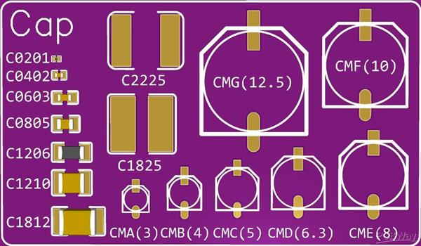
Three Main Areas of Environmental Regulations for Electronic Assembly
The Importance of Material Selection
Since 1995, certain cleaning agents used to clean substrate materials during assembly—such as Freon and trichloroethane—have been explicitly banned by the international community because they damage the Earth’s ozone layer. In addition, materials used in some assembly processes—such as lead (Pb), volatile organic compounds (VOCs), and resin-based circuit boards—also pose environmental challenges. When it comes to material selection, environmental considerations have become a factor that cannot be ignored.
Assembly technologies based on Sn-Pb soldering, such as fine-pitch QFP (Quad Flat Package), have made significant progress in single-pass reflow technology. However, transitioning to lead-free soldering now requires a comprehensive reassessment of various aspects, including the composition of solder materials, manufacturing processes, and reliability—a daunting task.
Advanced: How Environmental Requirements Influence Material Selection
The original text points out that since 1995, cleaning agents such as Freon and trichloroethane have been explicitly banned by the international community; materials such as lead, volatile organic compounds, and resin-based circuit boards also pose environmental challenges, making environmental considerations an indispensable factor in material selection. This shift has expanded the evaluation of materials beyond mere performance and cost to include the dimension of compliance.
| Controlled Materials | Environmental issues highlighted in the original text | Corresponding alternative directions |
|---|---|---|
| Freon Cleaner | Depletion of the ozone layer | Switch to alternatives such as HCFCs, HFCs, PFCs, and IPA |
| Trichloroethane | Both are classified as prohibited cleaning agents | To be phased out along with Freon |
| Lead (Pb) | Heavy Metal Pollution | The Shift to Lead-Free Soldering and Sn-Based Alloys |
| VOC | Emissions Harm the Environment and Human Health | Switch to a closed-loop recycling system and water-soluble materials |
| Resin Series Wiring Boards | Facing similar environmental challenges | Recyclability and degradability must be evaluated. |
The most important thing to keep in mind is"Substitutes themselves may also give rise to new environmental problems.". The original text explicitly states that alternatives such as HCFCs, HFCs, PFCs, and IPA still pose environmental concerns, which is why research and development of third-generation CFCs is still ongoing. This indicates that switching to environmentally friendly alternatives is often not a one-time transition, but rather an ongoing process of iteration; therefore, when selecting alternatives, it is important to allow for the possibility of future adjustments.
- First, check the exclusion list: Re-evaluate each material currently in use;
- Substitutes Must Undergo Environmental Review: The original text points out that they also have problems;
- The Reliability of the Transition to Lead-Free Must Be Re-evaluated: The original text refers to it as a daunting task;
- Compliance and performance must both be met: It is not enough to satisfy just one of them.
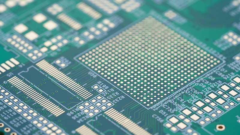
See "Lead-Free Process"The Application of Lead-Free Processes in PCB Manufacturing; For lead-free reliability analysis, seeReliability Analysis and Solutions for Lead-Free HDI Digital Products。
Challenges and Solutions for Lead-Free Soldering
The challenges associated with lead-free soldering include:
- Development of Alternative Welding Fluxes: Finding solder alternatives to lead is a critical task. These solders must meet multiple requirements, including low cost, a melting point close to that of Sn-Pb, superior electrical, mechanical, and chemical properties, compatibility with existing processes and equipment, and suitability for fine patterns.
- New Assembly Techniques: Lead-free soldering requires new assembly techniques and equipment. This means reevaluating existing joining techniques and developing new methods.
Advanced: Why Lead-Free Soldering Is a Challenging Task
The original text categorizes the challenges of lead-free soldering into two types: the development of alternative fluxes, and new assembly technologies and equipment. The former requires low cost, a melting point close to that of Sn-Pb, superior electromechanical and chemical properties, compatibility with existing process equipment, and suitability for fine patterns; the latter implies a reassessment of existing joining technologies.
| Evaluation Dimensions | Requirements in the original text | The Cost of Switching |
|---|---|---|
| Cost | Low-cost | Alloy Formulations and the Supply Chain Need to Be Rebuilt |
| Melting Point | Close to Sn-Pb | A high melting point will increase the welding temperature. |
| Electrical Properties | Superior | Continuity and reliability testing must be repeated. |
| Mechanical Properties | Superior | The strength and fatigue life of the welds must be retested. |
| Process Compatibility | Compatible with existing equipment | The furnace temperature curve and the flux must be adjusted simultaneously. |
| Detailed Graphics | Suitable for detailed graphics | Risks Associated with Fine-Pitch QFPs and Other Devices Are on the Rise |
The real challenge lies in"The Ripple Effects of Melting Point Shift". The original text mentions that significant progress has been made in one-pass reflow technology for fine-pitch QFPs based on Sn-Pb soldering; however, after switching to lead-free solder, the composition of the solder, the process, and reliability must all be reevaluated. An increase in melting point will simultaneously affect the oven temperature profile, the device’s thermal margin, and the appearance of the solder joints—this cannot be resolved simply by changing the alloy.
- First, evaluate the device's thermal margin.: An increase in melting point will reduce the allowance;
- Adjust the furnace temperature profile again: Compatible with the alloy's properties;
- The reliability of the solder joints must be retested.: Emphasis in the original text;
- Fine-pitch devices pose the highest risk: Requires thorough verification.
- Determine the melting point and process window of the alternative alloy;
- Verify the maximum temperature rating of the components on the board;
- Adjust the reflow profile and perform a first-article verification;
- Re-test the strength and appearance of the solder joints;
- Mass production will begin after the reliability tests are completed.
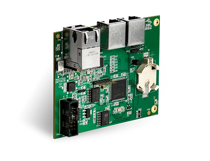
For an analysis of welding defects, seeAnalysis of SMT Soldering Defects and Solutions; For information on distinguishing between leaded and lead-free solder joints, seeHow to Determine Whether Solder Joints on a PCBA Board Are Leaded or Lead-Free。
Developments in New Assembly Materials and Technologies
1. Completely phase out the use of Freon
Freon is a cleaning agent used for circuit boards in assembly, but it damages the Earth’s ozone layer and contributes to global warming. The international community has restricted its use and banned Freon. It has been replaced by alternatives such as HCFCs (transitional compounds), HFCs (hydrofluorocarbons), PFCs (perfluorometaborane), IPA (isopropyl alcohol), propanol, and hexyl acetate. However, these alternatives also pose environmental concerns, so research and development of third-generation CFCs is actively underway.
2. Lead-Free Soldering Is on the Agenda
Due to the heavy metal contamination—including lead—caused by Sn-Pb soldering, the development of lead-free soldering technologies has become urgent. Researchers are actively developing Sn-based alloys, such as Sn-Ag alloys, to replace traditional Sn-Pb soldering. These alloys have already begun to be used in electronic products, where they maintain good soldering quality while improving environmental sustainability.
3. Development of Solderless Connection Technology
As electronic components continue to shrink in size and pin pitches become increasingly narrow, traditional soldering techniques can no longer meet the demands. Consequently, solder-free bonding technologies have begun to attract attention. These technologies include methods such as ultrasonic bonding and hot-press bonding, which allow IC chips to be bonded directly to substrate electrodes without the use of solder. This not only simplifies the process but also reduces the number of cleaning steps.
4. Control the Use and Emissions of VOCs
Controlling the use and emissions of volatile organic compounds (VOCs) is also an important aspect of environmental protection. This includes restricting the use of VOCs to enclosed or recoverable systems and developing new materials, such as water-soluble fluxes and flux-free resins, to reduce VOC usage. However, research on VOC control is still ongoing, as these compounds are diverse and exhibit varying properties.
Advanced: Why Is Detergent Replacement an Ongoing Process?
The original text explains that Freon, when used as a cleaning agent for wiring boards during assembly, damages the ozone layer and contributes to global warming, and the international community has restricted and banned its use, replacing it with alternatives such as HCFCs, HFCs, PFCs, IPA, propanol, and ethyl acetate. However, these alternatives also pose environmental concerns, so research and development of third-generation CFCs is currently underway.
- First-generation CFCs have been completely banned.: The original text explicitly states that the timeframe begins in 1995;
- Second-generation alternatives still pose an environmental burden: This should not be considered a final solution;
- The third generation is still under development.: It is necessary to continuously monitor changes in regulations;
- The no-wash process is another viable option: This can reduce the amount of detergent used.
The practical conclusion that follows from this is"Reducing the need for cleaning is a more fundamental solution than changing the cleaning agent.". The original text, in discussing flux-free joining technology, noted that it simplifies the process and reduces the number of cleaning steps. When the joining process itself no longer produces residues that require cleaning, reliance on cleaning agents naturally decreases—a more sustainable approach than constantly searching for more environmentally friendly solvents.
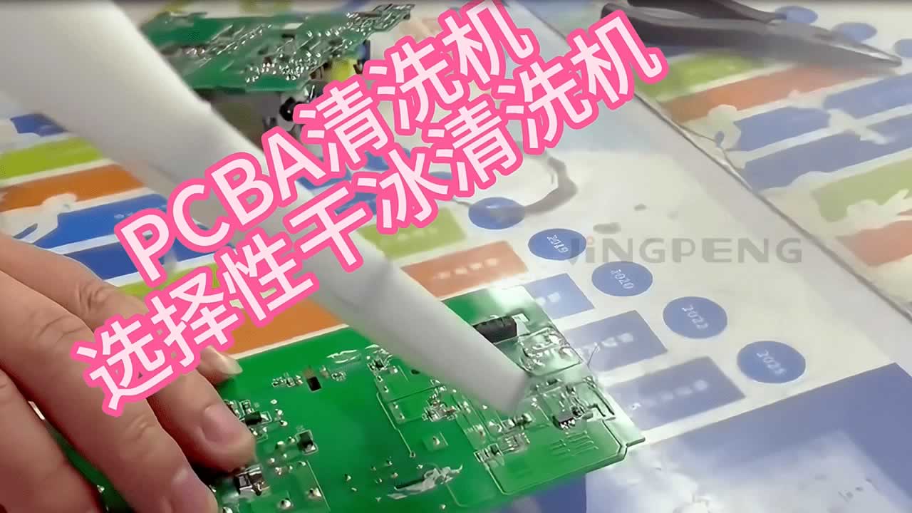
For cleaning instructions, seePCB Cleaning Methods; For the cleaning process, seePCB Cleaning; For selective soldering, seeSelective Soldering。
Conclusion
Driven by environmental pressures, the electronics assembly industry is actively seeking more environmentally friendly materials and technologies. Lead-free soldering, flux-free joining technologies, and the control of VOC use and emissions are all key issues at present. In the future, we can expect more environmentally friendly innovations to ensure the sustainability and environmental responsibility of electronic products.
Advanced: What Makes VOC Control So Challenging?
The original text identifies the control of the use and emissions of volatile organic compounds (VOCs) as a key aspect of environmental protection. Specific measures include restricting the use of VOCs to enclosed or recovery systems and developing new materials—such as water-soluble fluxes and flux-free resins—to reduce their consumption. The text also notes that research in this area is ongoing, given the wide variety of such compounds and their differing properties.
| Control Path | Original Method | Implementation Challenges |
|---|---|---|
| System Shutdown | Restricted to use in closed or recoverable systems | Equipment upgrades require a significant investment. |
| Material Substitution | Development of Water-Soluble Flux | Welding performance must be revalidated. |
| Material Substitution | Development of Solvent-Free Resins | Limited range of applicable processes |
| Reduction at the Source | Reduce VOC usage | Emissions must be calculated for each process step. |
| Ongoing Research | The original text notes that the research is still ongoing. | There is a wide variety of compounds, and their properties vary greatly. |
The root cause of the problem is"VOCs are not a single substance but a broad class of compounds.". The original text clearly states that there are many different types with varying properties, which means it is impossible to address emissions issues across all processes with a single, universal substitute; instead, solutions must be sought separately for each process. For this reason, related research is still ongoing.
For electrical reliability, seeEnsuring Electrical Reliability in PCBA Product Design; For information on solderability optimization, seeThe Impact of PCB Via Solderability on Soldering Quality and Optimization Methods。
Advanced: Limits of Application for Solderless Connection Technology
The original text explains that as components become smaller and pitch distances decrease, traditional soldering techniques can no longer meet the demands. As a result, solderless bonding technologies—including ultrasonic bonding and hot-press bonding—have garnered attention. These methods allow IC chips to be bonded directly to substrate electrodes without the need for solder, thereby simplifying the process and reducing the number of cleaning steps.
- Suitable for applications with extremely tight spacing: The driving factors identified in the original text;
- No flux is required, which reduces the need for cleaning: Consistent with environmental goals;
- Ultrasonic bonding and hot-press welding are the most common methods: The original text is listed below;
- High barriers to entry in terms of equipment and processes: The feasibility of mass production needs to be evaluated.
- Verify whether the device spacing exceeds the capabilities of conventional soldering;
- 评估超声键合或热压焊的适用性;
- 核对基板电极的可连接性;
- 验证连接可靠性与返修可行性;
- 确认批量生产的设备与节拍。
需要权衡的是「工艺简化与设备投入之间的取舍」。无焊剂连接省掉了焊剂与清洗两步,但引入了对设备精度和基板电极状态的更高要求。对产量大、间距极小的产品,这笔投入通常值得;对常规间距的产品,传统焊接仍是更经济的选择。

高可靠PCB特征见10 Characteristics of Highly Reliable PCBs; For assembly and testing, seeWhy Is PCB Assembly and Testing Necessary?。
Frequently Asked Questions
1. 无铅焊接是否会影响电子产品的性能?
无铅焊接已经取得了显著进展,可以提供与传统焊接相媲美的性能。因此,它不会显著影响电子产品的性能。
2. 为什么要废除使用氟里昂?
氟里昂会破坏地球的臭氧层,导致地球变暖。因此,国际社会采取了禁止使用氟里昂的措施。
3. 无焊剂连接技术是否安全?
无焊剂连接技术是安全的,并且在一些电子产品的制造中已经得到应用。它不涉及有害的焊剂,有助于减少环境污染。
4. 为什么要控制VOC的使用与排放?
VOC是有害的挥发性有机化合物,对环境和人类健康有害。因此,控制其使用与排放对环保至关重要。
5. 未来的电子组装趋势是什么?
未来的电子组装趋势包括更环保的材料和技术的发展,以及对电子产品的可持续性的关注。环保将继续推动创新和改进。
在面对电子组装的环保挑战时,我们需要不断努力,以确保电子产品的制造更加环保和可持续。同时,新的材料和技术的发展也将推动电子组装领域迈向更加可持续的未来。让我们共同关注环保,为地球的未来出一份力。
6. 无铅焊接切换时需要重新评估哪些内容?
原文指出从Sn-Pb焊接改为无铅焊接,需要重新评估焊接材料的组成、工艺和可靠性等多个方面。具体来说包括替代合金的熔点与工艺窗口、板上器件的耐热上限、回流温度曲线,以及焊点的机械强度与疲劳寿命。
7. 氟里昂的替代品是否完全环保?
并非完全环保。原文明确提到HCFC、HFC、PFC、IPA、丙醇和乙酸已脂等替代品同样存在环境问题,因此第三代CFC的研发正在积极进行。替代是一个持续迭代的过程,而不是一次完成的切换。
8. 减少VOC用量有哪些可行路径?
原文给出的路径包括把VOC的使用限制在封闭或可回收的系统中,以及开发水溶性焊剂和无熔剂树脂等新材料来减少用量。由于这类化合物种类繁多、性能各异,通常需要按工序分别寻找方案。
Related Recommendations:元器件短缺如何影响电子产品设计以及避免 · The Widespread Use of Ceramic Substrates in the New Energy Automotive Sector
