

In the world of modern technology, the printed circuit board (PCB) is hailed as the ”mother of all electronic products.” It serves as the connection point for electronic components, providing the foundation and interconnectivity necessary for the operation of electronic devices. This article will delve into the basic structure of PCBs, their importance in the 5G era, and the related technological advancements.
The Role of the Antenna Board in the RF Link
The antenna board serves as the interface between the feed network, the array elements, and the RF front end; it must not only transmit signals but also ensure stable amplitude correlation among the various channels. For issues related to the copper plating process, please refer toIssues with the Fifth-Generation Copper-Plating Process for Telecommunications。
Unlike standard digital boards, its key performance metrics focus more on loss, phase consistency, and impedance continuity. Any variation in dielectric thickness or copper surface topography can be amplified during the array calibration process; therefore, material and process consistency are often prioritized over routing density.
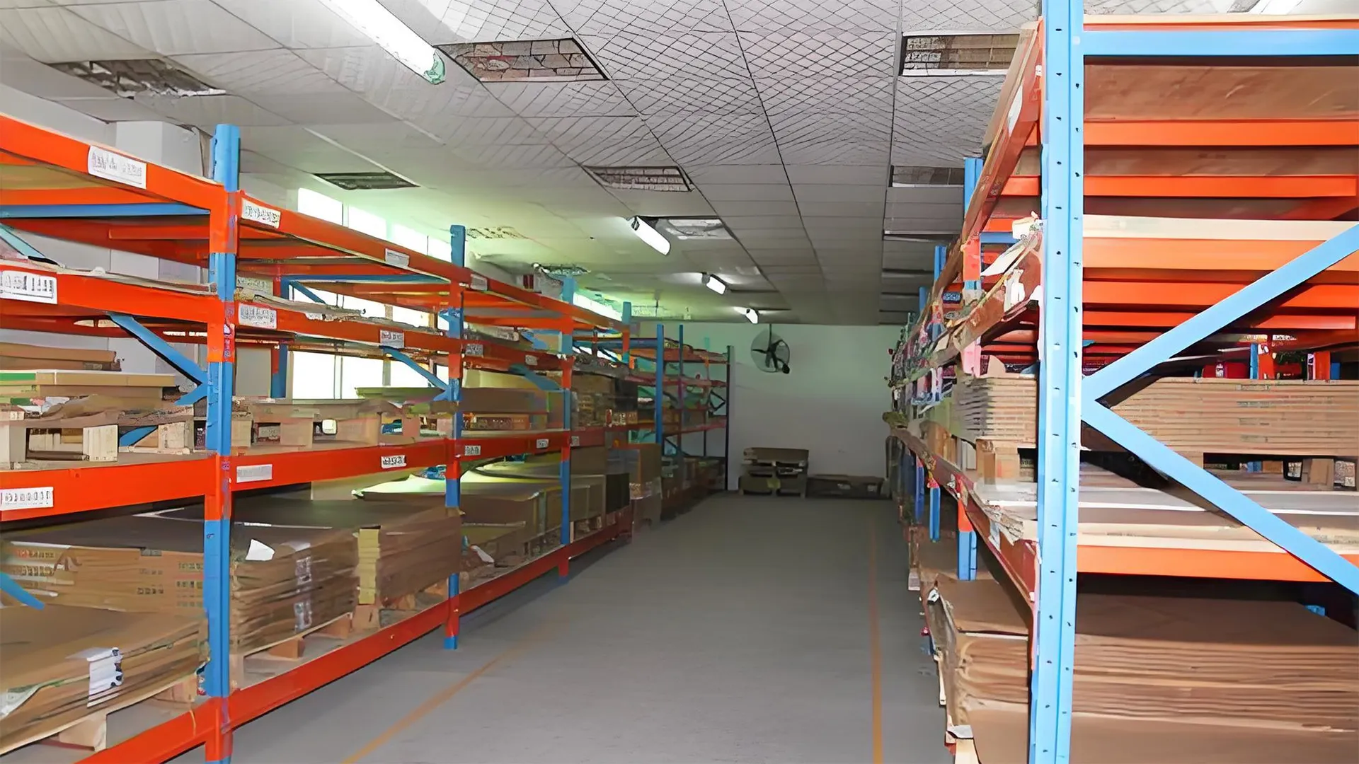
- Responsible for power distribution and interconnection.
- The correlation must be stable.
- The focus is on the loss phase.
- Impedance continuity is key.
- Fluctuations in the medium will be amplified.
- Consistency takes precedence over density.
Material Requirements Resulting from the Increase in Frequency Band
As the operating frequency increases, the impact of dielectric loss and conductor loss on the link budget becomes significantly greater, making the stability of a material’s dielectric constant and its loss factor key considerations in material selection. For reference, see the management guidelines.Fifth-Generation Communication Board Management Specifications。
At the same time, attention must be paid to moisture absorption: a material’s dielectric parameters may drift after absorbing water, which is particularly noticeable in outdoor or high-humidity environments. Evaluations should be based on actual measurement data within the operating frequency band, rather than simply comparing values at a single frequency point listed in a data sheet.

- It is more sensitive to dielectric loss.
- The dielectric constant must be stable.
- The loss factor has become the main focus.
- Moisture absorption can cause parameter drift.
- See the actual test results within the frequency band.
- A single data point is not sufficient evidence.
Drivers of Growth in Floor Area and Number of Stories
Large-scale arrays require more independent channels and feed paths; an increase in the number of elements directly increases the board area and the number of routing layers. For selecting high-frequency microwave boards, refer toSelecting High-Frequency Microwave Boards。
However, increasing the number of layers lengthens the production process, lowers the overall yield rate, and makes it easier for interlayer alignment errors to accumulate. The proper approach is to first optimize the partitioning and layer allocation, and only consider adding layers after confirming that isolation and routing requirements cannot be met with the current number of layers.

- The number of channels increases the area.
- The feed paths are more densely packed.
- The number of layers increases accordingly.
- The production process chain has been extended.
- Alignment errors can accumulate.
- Optimize first, then add layers.
The Impact of Array Structures on Layout
The element spacing, feed symmetry, and the routing of the calibration network collectively determine amplitude and phase consistency; therefore, the path lengths and number of layer transitions for each channel must be incorporated into a unified plan during the layout phase. For the selection of high-frequency materials, refer toSelection of High-Frequency Materials。
If a channel changes layers multiple times or takes a detour to avoid interference, the resulting phase deviation will be directly incorporated into the beamforming results. Therefore, symmetry and equal length are generally prioritized over local routing convenience, and adjustments should be made to the entire group rather than modifying individual channels.

- Plan the spacing and symmetry first.
- Path lengths must be consistent.
- The number of level changes affects the phase.
- Bypass deviation into the beam.
- Equal length takes precedence over convenience.
- Coordinated adjustment of the entire set.
High-Frequency Loss and Dielectric Stability
High-frequency losses result from a combination of dielectric loss, conductor loss, and radiation loss; the roughness of the copper foil, the type of surface treatment, and the solder mask coverage all contribute additional effects. For high-frequency design techniques, refer toHigh-Frequency Design Techniques。
Therefore, low-loss materials are only one part of the solution; if the copper surface is rough or the surface treatment is inappropriate, the benefits may be offset. The link budget should list the losses for each section separately and be verified through actual measurements on prototypes, rather than relying solely on upgrading materials.

- There is more than one source of loss.
- The roughness of the copper foil has an effect.
- Surface treatments also provide bonuses.
- Materials are just one part of the process.
- List the link budgets by segment.
- Confirmed through actual testing of the sample.
Layer Stacking and Impedance Matching
RF traces are typically impedance-controlled networks, and the combination of dielectric thickness, trace width, and distance from the reference plane must be determined once during the layer planning stage. To determine the number of layers, refer toDetermining the Number of Floors。
Fluctuations in dielectric thickness and material parameters between batches directly result in impedance dispersion; therefore, it is essential not only to review the design values but also to verify the consistency of incoming materials and the production line’s control capabilities. A complete reflow path is also required at layer transitions; otherwise, discontinuities will cause reflections.
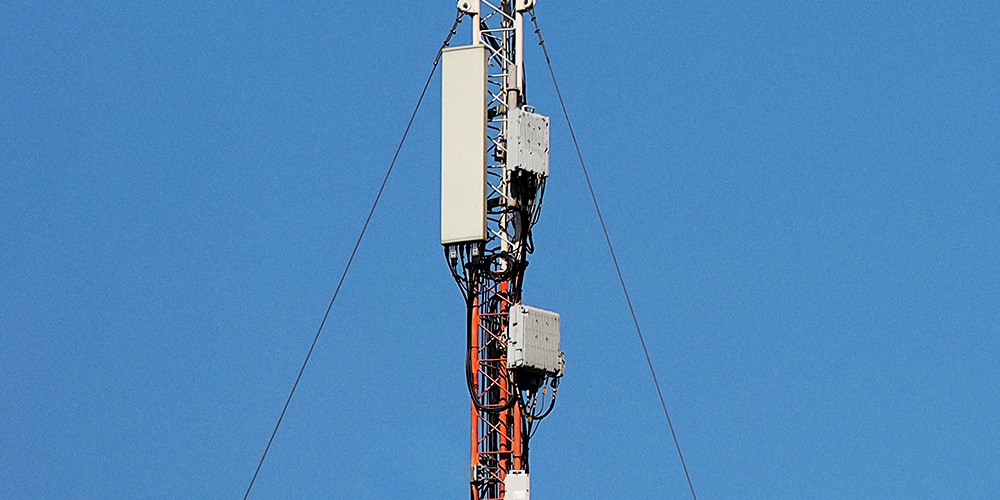
- Get the layering right the first time.
- The thickness of the medium is key.
- Batch-to-batch variations lead to dispersion.
- The consistency of incoming materials must be verified.
- The layer-to-layer backflow must be complete.
- Discontinuities will cause reflections.
Heat Dissipation and Power Density
RF front-end devices operate in a confined space, and an increase in power density can alter material properties and affect the long-term reliability of solder joints; therefore, thermal management must be considered in tandem with electrical design.
A common approach is to use the entire copper surface, thermally conductive vias, and metal heat dissipation structures to establish a low-thermal-resistance path; however, interface contact, voids in the solder layer, and the heat dissipation conditions of the enclosure also determine the final temperature rise, so simply switching to a highly thermally conductive material does not necessarily solve the problem.
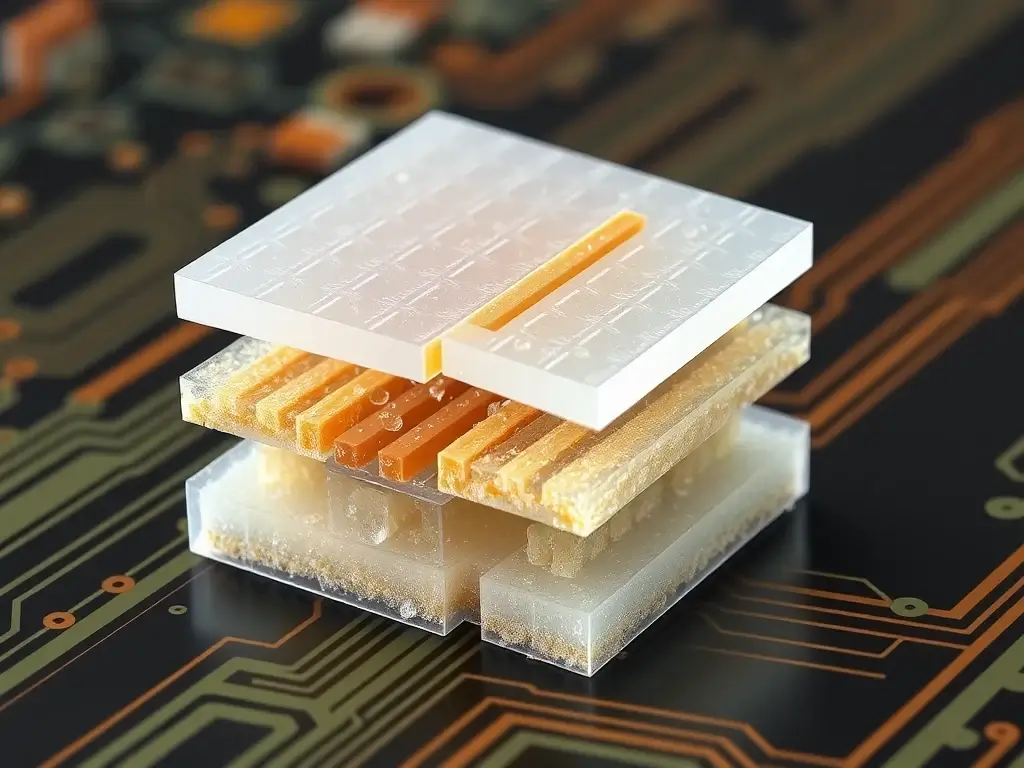
- Power density has increased.
- Adjust the material parameters based on the temperature rise.
- Affects the reliability of the solder joints.
- Copper surfaces and heat-conducting holes are commonly used.
- Interface thermal resistance cannot be ignored.
- Changing the material doesn't mean the problem is solved.
Manufacturing Precision and Yield Rate
When fine lines, small vias, and a high number of layers are combined, the tolerance windows for etching accuracy, interlayer alignment, and plating uniformity become significantly narrower, making the manufacturing process more challenging than that of standard boards with the same number of layers.
Moving inspection points to before critical stages and retaining data on first-article and batch trends is more effective than conducting centralized inspections just before shipment. For critical characteristics, acceptance criteria and sampling levels should also be clearly defined to avoid differing interpretations of the same defect between the supplier and the customer.
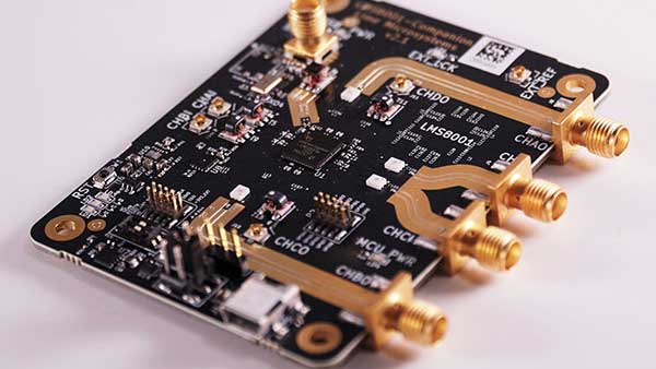
- The process window is narrower.
- Etching alignment must be controlled.
- It relates to coating uniformity.
- Testing sites should be moved forward.
- Trend data is more reliable.
- The acceptance criteria are specified.
Testing and Validation Methods
Electrical verification typically includes tests such as impedance, insertion loss, return loss, and phase consistency, each of which reflects the quality of different aspects of the system and cannot be substituted for one another.
Test conditions must be standardized, and the ambient temperature, fixture configuration, and calibration status must be recorded; otherwise, data across different batches cannot be compared. For array-type boards, attention must also be paid to the consistency of distribution across channels, rather than simply whether a single link meets the standards.
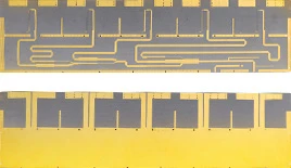
- Measure impedance, insertion loss, and return loss simultaneously.
- Phase consistency is key.
- The methods are not interchangeable.
- The conditions must be recorded consistently.
- See the notes regarding fixture calibration.
- Look at the distribution across the channels.
Cost and Supply Constraints
Low-loss materials, high layer counts, and more stringent testing requirements all contribute to higher costs and longer lead times, and supply stability has also become a key consideration in the selection process. For trends in the materials industry, please refer toIssues with the Fifth-Generation Copper-Plating Process for Telecommunications。
The evaluation should include a full-cost comparison: factors such as yield rates, specialized tooling, testing hours, and batch consistency risks should all be taken into account. If the product’s operating frequency is not high or there is sufficient link margin, using a generic system combined with stacking optimization is often more cost-effective than a comprehensive material upgrade.
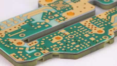
- The number of material layers is also increasing.
- Delivery time must also be taken into account.
- Supply stability is important.
- A full-cost comparison is the only accurate way to evaluate this.
- Yield rates and tooling costs must both be taken into account.
- There is plenty of leeway, so there's no need to meet the high standards.
Comparison of Changes in Demand
Comparing changes in frequency bands, array size, and manufacturing requirements side by side helps determine which upgrades are necessary during the proposal review process. The table below provides only a qualitative summary.
The table does not serve as a substitute for any link budget or material data sheet. Specific selections should be based on device specifications, applicable standards, actual test results of samples, and supplier capability documentation, and should be verified in conjunction with on-site process capabilities.
| Demand Dimensions | Key Changes | Design Solutions |
|---|---|---|
| Operating Frequency Band | More sensitive to losses | Selection of Low-Loss Materials |
| Array Size | Increase in Channels and Levels | Symmetry and Layered Planning |
| Manufacturing Requirements | The process window is narrowing | Moving Testing Locations Upstream |

- The form is used for proposal review.
- It is merely qualitative induction.
- This does not replace the link budget.
- Device specifications take precedence.
- The results of the actual test serve as further evidence.
- Verify production line capacity.
Design Evaluation Checklist
We recommend verifying the following items one by one: operating frequency band and link margin, dielectric parameter stability, array channel symmetry, stacking and impedance schemes, heat dissipation paths, test items, and supply and cost constraints. For material selection, please refer toSelection of High-Frequency Materials。
The checklist should be updated along with sample and mass-production data, incorporating measured loss, impedance variation, and yield trends as the basis for the next round of component selection. This ensures that upgrade decisions are supported by quantifiable data, rather than simply proceeding with the assumption that “a new generation must use better boards.”
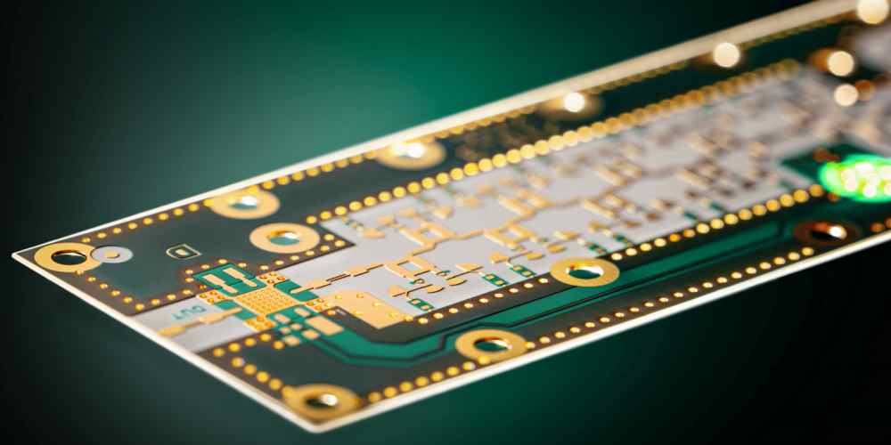
- First, confirm the frequency band margin.
- Dielectric stability is crucial.
- Channel Symmetry Check.
- Heat dissipation testing is listed in the same column.
- There are limits to supply costs.
- Write back the actual test data.
Frequently Asked Questions
1. Why does material selection become more critical as the frequency increases?
Because dielectric loss and conductor loss have a significantly greater impact on the link budget as frequency increases, the stability of the dielectric constant is directly related to impedance and phase consistency, while the loss factor determines how much energy is converted into heat. In addition, material parameters may drift when the material absorbs moisture, which is particularly noticeable in outdoor or high-humidity environments. Evaluations should be based on actual measurement data across the entire operating frequency range, rather than simply comparing values at a single frequency point listed in a data sheet.
2. Why do large-scale arrays increase the number of layers and the area?
An increase in the number of array elements means more independent RF channels and feed paths; since the spacing between elements must meet electromagnetic design requirements, the board area naturally increases, and routing space becomes more constrained, often requiring additional layers to accommodate traces and reference planes. However, adding layers lengthens the manufacturing process, lowers the overall yield, and accumulates interlayer alignment errors. Therefore, you should first optimize the partitioning and stackup configuration and only add layers after confirming that the current number of layers is indeed insufficient.
3. Will switching to low-loss materials definitely ensure that loss meets the standard?
Not necessarily. High-frequency losses result from a combination of dielectric loss, conductor loss, and radiation loss; additional losses can be caused by copper foil roughness, the type of surface treatment, solder mask coverage, and discontinuities at layer transitions. Materials are only one factor; if the copper surface topography or layer stackup is inappropriate, the benefits of upgrading may be offset. The recommended approach is to break down the link budget into segments and identify the primary sources of loss through actual measurements on prototypes.
4. Why does array layout place such a strong emphasis on symmetry and equal lengths?
The amplitude correlation between channels directly determines the beamforming results. If a channel changes layers multiple times or takes a detour to avoid interference, the resulting phase deviations will be introduced into the synthesis and are difficult to fully compensate for later using software. Therefore, element spacing, feed symmetry, and the number of layer changes should be planned uniformly during the layout phase, with equal lengths taking precedence over local routing convenience; when adjustments are necessary, they should be made to the entire group rather than modifying a single channel individually.
5. What are the main factors that affect impedance matching?
The characteristic impedance is determined by the combination of dielectric thickness, line width, copper thickness, and distance from the reference plane; these parameters must be established once during the lamination stage. Fluctuations in dielectric thickness and material parameters between batches directly result in impedance dispersion; therefore, in addition to design values, it is essential to verify the consistency of incoming materials and the production line’s control capabilities. If the return path is incomplete at layer transitions, discontinuities may form, leading to reflections.
6. Why can’t heat dissipation for antenna boards be determined solely by the board material?
RF front-end devices operate in a confined area; an increase in power density can alter material properties and affect the long-term reliability of solder joints. Solid copper layers, thermally conductive vias, and metal structures can establish low-thermal-resistance paths; however, interface contact, voids in the solder layer, case heat dissipation, and airflow also determine the final temperature rise. If the bottleneck lies at the interface or in the case, simply replacing the board with one made of highly thermally conductive material often fails to produce the expected results.
7. Why must the test conditions for these types of boards be fixed?
Readings for impedance, insertion loss, return loss, and phase consistency are affected by ambient temperature, fixture condition, and calibration methods. When conditions are not consistent, data across batches cannot be compared, and trend analysis becomes meaningless. For array-type boards, attention should also be paid to the consistency of distribution across channels, rather than merely whether a single link meets the specifications. Test records should include calibration information, fixture numbers, and environmental conditions.
8. How can you determine whether upgrading the materials and the number of layers is worth it?
A comprehensive cost comparison should be conducted: low-loss materials, high layer counts, and more stringent inspection requirements will drive up the unit price; yield losses, specialized tooling, testing labor hours, and delivery time risks must also be factored in; supply stability is another key consideration. If the operating frequency is not high or the link margin is sufficient, using off-the-shelf materials combined with stack-up and routing optimization is typically more cost-effective. The final decision should be based on link budget, actual prototype testing, and mass production yield—not generational labels.
Basic Structure of a PCB
PCBs are primarily composed of two materials: insulating substrates and conductors. As a composite material used to connect various electronic components—from tiny transistors to complex microprocessors—PCBs play a crucial role. Different PCB structures include rigid boards, flexible boards, and rigid-flex boards, and based on the number of layers, they can be classified as single-sided, double-sided, and multilayer boards.
The Major Changes Brought About by 5G
The rise of 5G technology willBase StationThis has brought about significant changes in the architecture, with PCBs playing a key role. In the 4G era, a standard macro base station consisted of three components: the baseband processing unit (BBU), the radio frequency processing unit (RRU), and the antenna. However, with the advent of 5G, traditional CPRI connections no longer provide sufficient transmission bandwidth, necessitating a redesign of the 5G base station architecture.
In 5G base stations, due to the need for Massive MIMO antenna technology, some of the BBU’s functions are integrated with the RRU and antennas to form a new Active Antenna Unit (AAU). The remaining BBU functions have been split into a two-tier architecture consisting of the CU and DU. The DU (Distributed Unit) is responsible for meeting real-time requirements and also handles some low-level baseband protocol processing; the CU (Centralized Unit) handles non-real-time high-level wireless protocol processing.
PCB Upgrade
The antenna arrays in 5G base stations require highly advanced PCB technology. Compared to the 4G era, 5G PCBs have been upgraded in several ways:
1. Increase in PCB area and number of layers
In the 4G era, antenna arrays typically consisted of no more than 8 antennas, whereas 5G antenna arrays can include up to 192 antennas, forming a Massive MIMO antenna array. This results in a significant increase in the PCB area required.
2. Increased Complexity
Due to the significant increase in communication channels, PCBs in the 5G era require more complex designs, evolving from the double-sided boards of the 4G era to 12-layer boards. This increased complexity demands a higher level of technical expertise in both PCB manufacturing and design.
3. Material Upgrades
In the 5G era, PCBs require high-frequency, high-speed laminates to meet signal transmission requirements. This has also led to a significant increase in the value of PCBs.
The rise of 5G technology will greatly drive the development and innovation of PCB technology. PCBs are no longer merely connectors for electronic devices; they have become a vital component supporting 5G communications and the technological revolution. In the future, we can expect PCB technology to play a key role in more fields, driving the continuous advancement of electronic technology.
Frequently Asked Questions:
- Question: What is the role of a PCB in electronic devices?Answer: A PCB serves as the medium for connecting electronic components; it supports and interconnects various electronic components and is a fundamental component of electronic devices.
- Question: Why is it necessary to upgrade PCB technology in the 5G era?Answer: 5G introduces Massive MIMO and higher communication frequencies, requiring larger, more complex, and higher-performance PCBs to support these new technologies.
- Question: How do the number of layers and the area of a PCB affect its performance?Answer: The number of layers and the area of a PCB determine its signal transmission capabilities and complexity, which are closely related to the performance of electronic devices.
- Question: How does the choice of PCB material affect performance?Answer: The choice of PCB material affects its signal transmission characteristics and durability, and has a significant impact on its performance.
- Question: What are the trends in PCB technology?Answer: PCB technology will continue to evolve toward higher density, higher frequency, higher speed, and greater versatility to meet the demands of future electronic devices.
Additional Information:The Dangers of Counterfeit Electronic Components to PCBA · Future Trends in PCB Technology