

Printed circuit boards (PCBs) are the core components of all electronic devices,How Should You Choose Between HDI Boards and Standard PCBs?。
The differences between HDI (High-Density Interconnect) boards and traditional standard PCBs directly determine a product’s performance, size, and cost.
Whether it's high-end products such as smartphones and 5G devices or standard electronic devices, choosing the right type of PCB is crucial.
This article will provide a detailed explanation of the differences between the two and their applicable scenarios from five key perspectives—including materials, manufacturing processes, and performance—to help you quickly make a selection decision.
I. Differences in Core Materials: Determining the Upper Limit of a PCB’s Basic Performance
1. Standard PCB: FR-4 core, prioritizing cost-effectiveness
The most common base materials for standard PCBs areFR-4 Epoxy Resin Glass Cloth Substrate(Made by laminating electronic-grade glass cloth with epoxy resin).
It offers basic mechanical strength, insulation, and electrical properties, and is relatively inexpensive.
It meets the needs of most standard electronic devices (such as routers and control boards for common household appliances).
It is currently the most widely used PCB substrate.
2. HDI Boards: FR-4 + Specialty Materials, Designed for High-Density Applications
HDI boards can also use FR-4 substrate, but must be combined withFiberglass-Free Adhesive-Backed Copper Foil (RCC)。
The main reason is that HDI boards require “high-energy laser drilling technology” to achieve very small hole diameters (typically ≤0.15 mm).
Fiberglass-free adhesive-backed copper foil prevents burrs and resin residue during laser drilling, ensuring precise circuit connections.
This lays the material foundation for high-density circuits.
II. Differences in Manufacturing Processes: Layered Fabrication vs. Traditional Etching—A World of Difference in Complexity
1. Standard PCBs: Primarily single-layer or double-layer, with a simple manufacturing process
Standard PCBs typically use "traditional etching processes" and are primarily single-layer or double-layer boards.
Some multilayer boards also require only simple lamination, involving fewer process steps and a shorter production cycle.
There is no need for complex processes such as laser drilling or electroplating to fill holes, so manufacturing costs can be kept under control.
2. HDI Boards: Laminate Process + Advanced Technology; The Number of Layers Determines the Quality Grade
The core process for HDI boards is the “build-up” method, which involves stacking circuit layers one by one.
The higher the cumulative level, the higher the technical grade.:
Entry-Level HDI: 1 layer of lamination, basic laser drilling;
Advanced HDI: Two or more layers, combined with technologies such as "stacked vias, electroplated vias, and laser direct drilling (LDI)."
It can achieve ultra-fine lines (line width/line spacing ≤ 3 mil) and ultra-high layer counts (up to 20 layers or more).
The complexity and precision of the manufacturing process far exceed those of ordinary PCBs.
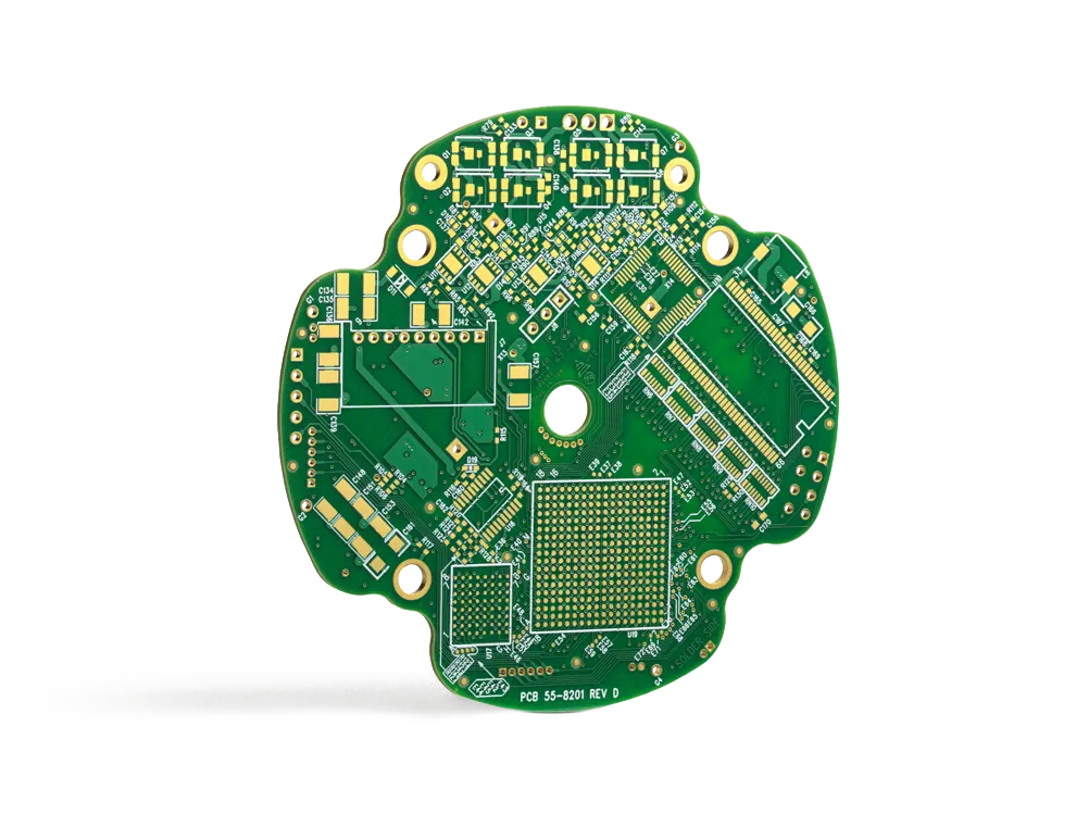
III. Circuit Density and Complexity: Key Selection Criteria for Miniaturized Products
1. Standard PCB: Low density, suitable for conventional layouts
Standard PCBs have a low trace density (trace width/spacing is typically ≥6 mil, and hole diameter is ≥0.3 mm).
It is not possible to fit a large number of electronic components into a limited space.
It is better suited for devices with modest size requirements and single functions (such as power strip control boards and simple sensors).
2. HDI Boards: High Density + High Integration, Enabling Product Miniaturization
The key advantage of HDI boards is their “high trace density.”
For the same area, the number of traces is 2 to 3 times that of a standard PCB, enabling high-density component integration.
This feature perfectly meets the demand for "smaller, lighter, and thinner" modern electronic products.
It is the PCB type of choice for high-end products such as smartphones, laptops, smartwatches, drones, and 5G base station equipment.
IV. Electrical Performance and Signal Reliability: Key Differences in High-Frequency, High-Speed Scenarios
1. Standard PCB: Basic electrical performance; not suitable for high-frequency, high-speed applications
Standard PCBs have wide trace spacing and large via diameters, making them susceptible to "radio frequency interference (RFI)" and "electromagnetic interference (EMI)" during signal transmission.
Furthermore, thermal conductivity is low, and signal delay and loss are quite significant.
It is only capable of supporting low-frequency, low-speed data transmission (such as control signals for ordinary household appliances).
2. HDI boards: Interference resistance + low loss—the top choice for high-frequency, high-speed applications
Thanks to ultra-fine traces, micro-via holes, and an optimized layer stackup design, HDI boards offer three key electrical performance advantages:
Immunity to Interference: Improved shielding performance against RFI, EMI, and electrostatic discharge (ESD) by more than 30%;
Signal Integrity: Signal transmission delay reduced by 20%; loss reduced by 15%–25%;
Heat Transfer Efficiency: The multi-layer stacked design accelerates heat dissipation and prevents high temperatures from affecting performance.
Therefore, HDI boards are more reliable in high-frequency applications (such as 5G communications and RF equipment) and high-speed data transmission scenarios (such as servers and solid-state drives).
V. Cost Variances: Balancing Performance and Budget
1. Standard PCBs: Low cost, excellent value for the price
Because standard PCBs use conventional materials and simple manufacturing processes, their cost per unit area is only 1/3 to 1/5 that of HDI boards.
Suitable for mass production of mid- to low-end products with modest performance requirements, it effectively controls overall production costs.
2. HDI boards: They are relatively expensive, but prices are clearly trending downward.
The high cost of HDI boards stems from two factors:
① Specialty materials (glass-fiber-free, self-adhesive copper foil) are more expensive;
② Processes such as laser drilling and electroplating to fill holes increase production lead times and equipment costs.
However, with the surge in demand for 5G and consumer electronics, as well as increased production capacity for HDI boards, costs have fallen by 15%-20% over the past three years.
The cost-effectiveness of bulk purchasing is becoming increasingly apparent.
Selection Conclusion: Precise Match Based on Requirements
| Dimensions of Comparison | Standard PCB | HDI Board |
|---|---|---|
| Core Strengths | Low cost, mature manufacturing process, and excellent value for money | High line density, strong interference resistance, and suitable for high-frequency, high-speed applications |
| Applicable Scenarios | Common household appliances, routers, and simple sensors | Smartphones, 5G devices, servers, drones |
| Selection Recommendations | Limited budget, single function, no need for miniaturization | Pursuing slim and lightweight designs, high performance, and high-frequency, high-speed data transmission |
Frequently Asked Questions
1. What is the key difference between HDI boards and standard PCBs?
The key differences boil down to three points:
① Materials(HDI includes glass-free, adhesive-backed copper foil);
② Process(HDI using the lamination method + laser drilling);
③ Performance(HDI offers higher circuit density and better interference resistance).
Standard PCBs place greater emphasis on value for money.
2. In which electronic products are HDI boards primarily used?
Major applications include smartphones, laptops, smartwatches, 5G base stations, servers, medical devices, drones, and other devices that require miniaturization and high performance.
3. Can standard PCBs be used in high-frequency, high-speed applications?
Not recommended.
Standard PCBs have wide trace spacing and poor immunity to interference; they suffer from significant signal loss during high-frequency (≥2 GHz) and high-speed (≥10 Gbps) transmission, making them prone to stuttering and bit errors.
4. Is a higher number of layers better for HDI boards?
Not necessarily.
The number of layers must match the product requirements:
One layer is sufficient for standard high-end smartphones, while two or more layers are suitable for complex devices such as servers and 5G base stations.
Excessive layering increases costs and puts pressure on heat dissipation.
5. When purchasing in bulk, how significant is the cost difference between HDI boards and standard PCBs?
For bulk purchases (≥1,000 pieces), the cost per unit area of HDI boards is approximately 2 to 3 times that of standard PCBs.
If you choose an entry-level HDI with a single layer, the cost difference can be reduced to about 1.5 times.
6. Why is FR-4 the most popular choice for PCB substrates?
FR-4 substrate combines good electrical insulation, mechanical strength, and temperature resistance, and is reasonably priced.
It meets the basic requirements for electronic devices rated at 80% or higher, making it the preferred base material for standard PCBs and entry-level HDI boards.
