

With the continuous advancement of science and technology—particularly information technology—the manufacturing processes for PCBs are also constantly improving to meet the needs of different users. In recent years, rapid development in sectors such as telecommunications and the automotive industry has led to a steady increase in demand for PCBs, particularly for high-power and high-frequencyMicrowave Boarddemand. Many PCB manufacturers are optimistic about this growth opportunity, but to successfully produce high-frequency microwave boards, companies must strengthen their core capabilities. This article will briefly outline the key considerations in the production of high-frequency microwave boards.
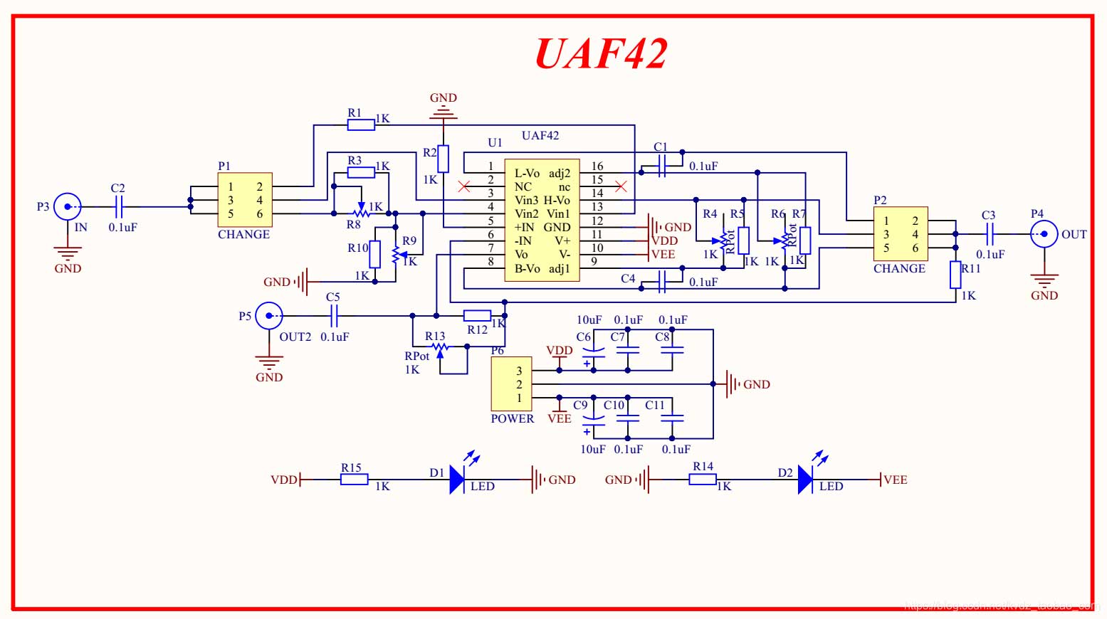
Advanced: What Makes High-Frequency Microwave Boards So Special?
When it comes to manufacturing printed circuit boards, the challenges associated with high-frequency microwave boards are concentrated in three areas:Dielectric properties of materials, dimensional accuracy of patterns, and microstructure of metal surfaces. If any one of these factors gets out of control, it will affect insertion loss and standing wave ratio.
| Key Features | Impact on RF Performance | Control Points in Production |
|---|---|---|
| Dielectric Constant (Dk) | Factors Affecting Impedance and Signal Propagation Speed | Material Batch Consistency, Stack-Up Thickness |
| Tangent of the loss angle (Df) | Factors Affecting Insertion Loss and Heat Generation | Material Selection and Avoiding Prolonged Processing at High Temperatures |
| Line Width Accuracy | Directly affects the characteristic impedance | Etch Compensation, Etch Uniformity |
| Wire Edge Morphology | Rough edges can increase wear and tear. | Etching Parameters, Copper Foil Types |
| Media Thickness Tolerance | Factors Affecting Impedance and Phase Consistency | Pressing Parameters and Selection of Pre-pregs |
- For standard circuit boards, check for continuity; for high-frequency circuit boards, check the dimensions.: For standard PCBs, it is sufficient for the continuity to be correct; for high-frequency PCBs, the trace width must also be within the tolerance range;
- The tolerance band is much narrower: While the line width tolerances for standard PCBs can be more lenient, high-frequency PCBs often require tolerances to be kept within a very narrow range;
- Batch consistency is more important: Achieving phase consistency across a batch of boards is often more difficult than meeting individual specifications.
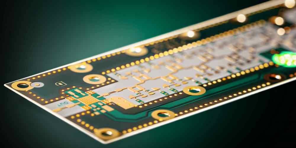
For key considerations in selecting high-frequency circuit boards, seeHigh-Frequency Microwave Board Selection Guide; For a description of high-frequency board characteristics, seeWhat Are High-Frequency, High-Speed PCBs?。
1. Processing of Engineering Data
When handling customer engineering documents, there are two key aspects to keep in mind. First, it is essential to thoroughly understand the manufacturing precision requirements for transmission lines, as these directly affect the performance of high-frequency microwave boards. Second, appropriate process compensation must be applied based on manufacturing capabilities and precision requirements. The accuracy of engineering data is critical to the production of high-frequency microwave boards.
2. Cutting
Typically, printed circuit boards are cut using shearing machines or automatic cutting machines; however, the situation is different for microwave dielectric materials. Depending on the specific properties of the dielectric material, different cutting methods must be selected—usually milling or cutting—to ensure the material’s flatness and the quality of the board surface.
3. Drilling
Different dielectric materials require different drilling parameters, and there are also specific requirements for the drill bit’s point angle, cutting edge length, and helix angle. For aluminum-based and copper-based microwave dielectric materials, different machining methods are used during drilling to prevent burrs from forming.
4. Grounding Through-Holes
Generally, through-holes are grounded using chemical copper plating. Chemical copper plating can be performed using either a chemical or plasma process. For aluminum-based microwave dielectric materials, it is typically recommended to ground the through-holes by filling them with a conductive metal material; however, the hole resistance should generally be less than 20 mm.
Advanced: Common High-Frequency Substrates and Processing Differences
The most commonly used substrate materials for high-frequency microwave boards vary greatly in their processing characteristics, so the process parameters for FR-4 cannot be directly applied:
| Material Type | Features | Processing Considerations |
|---|---|---|
| PTFE-based (including ceramic-filled) | Extremely low loss, stable Dk | The material is soft, and drilling can easily cause smearing, so special treatment is required. |
| Hydrocarbon Resin with Ceramic Filler | Low wear and better machinability than PTFE | Molding parameters must be adjusted according to the material specifications. |
| Modified Epoxy / High Tg FR-4 | Low cost and good workability | High-frequency loss is relatively high; suitable for the mid- and low-frequency ranges |
| Metal-Cored Microwave Boards | Good thermal conductivity; used for high-power applications | Cooling is necessary to prevent burrs during drilling and milling. |
- PTFE materials require surface activation: Since the bore wall is inert, it must undergo special treatment prior to electroless copper plating; otherwise, the bond strength will be insufficient;
- Drilling parameters must be adjusted individually.: Soft materials can easily cause damage to the bore wall, so both the drill bit geometry and the retraction rhythm must be adjusted;
- Higher pressing temperature: Since curing temperatures vary significantly among different materials, a compatible range must be selected when mixing and molding.
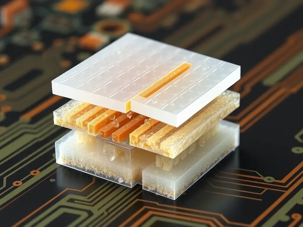
For storage requirements for high-frequency boards, seeStorage Requirements and Shelf Life of High-Frequency PCBs; See Notes on High-Frequency CablingPrecautions for Routing High-Frequency PCBs。
5. Graphic Transfer
Pattern transfer is a critical step in ensuring the precision of patterns on high-frequency microwave circuit boards. When selecting photosensitive materials such as photoresists, wet films, and dry films, it is essential that they meet the requirements for pattern precision. At the same time, the light source of the lithography or exposure system must also meet the needs of the manufacturing process.
6. Etching
During the etching process, process parameters must be strictly controlled, including the concentrations of the various components in the etching solution, the temperature of the etching solution, and the etching rate. This ensures that the edges of the conductors are clean and free of burrs and notches, and that the conductor dimensions remain within the required tolerance range.
7. Coating
The final coating on the conductors of high-frequency microwave boards typically consists of tin-lead alloys, tin-indium alloys, tin-strontium alloys, silver, gold, and other materials. However, electroplating with pure gold is a relatively common choice.
Advanced: What Exactly Does Process Compensation Compensate For?
The term “process compensation” mentioned in the engineering data processing refers toCorrecting dimensional deviations caused by etching in advance when producing graphics. Etching is isotropic; as the lines are etched downward, they are also etched laterally, resulting in a finished line width that is narrower than the design value.
- Determining the Amount of Side Erosion: Based on estimates derived from copper thickness and etching parameters, the thicker the copper, the greater the side etching tends to be;
- Widening the line width when doing light painting: Add back the estimated loss in advance;
- Calculate the target line width based on impedance requirements: The trace width on high-frequency boards is determined by impedance and must remain within the impedance window even after compensation;
- Fine-tune after testing the first unit: Measure the actual line width using cross-sectional analysis, and use this data along with the impedance test results to adjust the compensation value;
- Record and Reuse: The compensation factor for materials with the same copper thickness can be set as an empirical value.
Compensation on high-frequency boards is more sensitive than on conventional boards because deviations in line width directly translate into impedance deviations.A trace width variation of 10% on a standard PCB may not be an issue, but on a high-frequency PCB, it could exceed the impedance tolerance.. This is also why high-frequency boards rely more heavily on a closed-loop process involving first-article slicing and actual impedance measurements.
- Check both the top and bottom line widths: After etching, the cross-section takes on a trapezoidal shape, and the difference between the upper and lower widths serves as a measure of the amount of side etching;
- The difference between isolated-line and dense-line compensation: The amount of side etching varies depending on the etching solution replacement conditions;
- The distribution of graphics should be balanced.: Excessive variations in copper distribution can cause uneven etching, which in turn affects line width consistency.
For impedance and loss, seeThe Effects of PCB Impedance and Loss on Signals; For the basics of impedance, seeWhat Is PCB Impedance?。
8. Forming
The fabrication of high-frequency microwave boards is similar to that of printed circuit boards and typically involves CNC milling. However, milling methods vary significantly depending on the material; in particular, metal-based microwave boards require cooling with a neutral coolant, and the milling parameters also differ.
Advanced: What Specific Tests Are Required for High-Frequency Microwave Boards?
- Impedance Testing: Measuring the actual characteristic impedance using a TDR is the most direct way to verify performance;
- Insertion Loss and Return Loss: Measure S-parameters using a vector network analyzer to evaluate signal integrity and matching;
- Slice Analysis: Measure the line width, dielectric thickness, and copper thickness to verify that the geometric dimensions meet specifications;
- Peel Strength: For PTFE-based materials, the bond strength with copper foil must be thoroughly verified;
- Thermal Stress and Dielectric Strength: Verify the metallization and insulation reliability of the test holes.
Among these, insertion loss testing best reflects actual RF performance, but it is also the most expensive, so it is typically performed on a sample basis rather than on every unit. A common practice during mass production is:Full inspection of impedance, random sampling of insertion loss, and cross-section analysis for each batch...using these three results together to ensure quality.
- First-piece phase: Conduct full-project validation to confirm the process window;
- Batch Phase: Full inspection of impedance + random inspection of insertion loss + random inspection of cross-sections;
- Abnormal Phase: If any indicator drifts, return to the first-piece process and reconfirm.
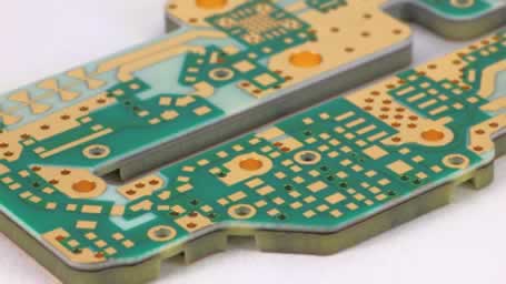
Key Points for Prototyping Automotive Rigid-Flex PCBs can be found atPoints to Consider When Prototyping Automotive Rigid-Flex Boards; For an overview of manufacturing capabilities, seePCB Manufacturing Capabilities。
In summary, every step in the production of high-frequency microwave boards requires special attention. Only by handling each stage with meticulous care can we ensure the production of high-quality products. High-frequency microwave boards represent a challenging field, but they also present greater opportunities for the PCB manufacturing industry.
Frequently Asked Questions
1. Why is the processing of engineering data so important?
The handling of engineering data affects the performance and quality of high-frequency microwave circuit boards; ensuring manufacturing precision and process compensation is key to guaranteeing product quality.
2. Why choose different cutting methods?
Different media materials have different properties, so it is necessary to select an appropriate cutting method to ensure material quality.
3. Why are through-holes grounded in different ways?
Different microwave dielectric materials require different grounding methods to ensure performance and quality.
4. Why is the selection of photoresist important in pattern transfer?
The choice of photoresist directly affects pattern accuracy and must meet process requirements.
5. Why are etching process parameters so important?
Controlling the etching process parameters ensures that the quality of the conductors meets requirements and prevents burrs and notches.
6. Can high-frequency boards and standard FR-4 boards be assembled together?
Yes, this is a hybrid laminate. The process involves using high-frequency materials in the RF region and lower-cost standard materials in other regions, with both laminated together in a single stack-up. The challenge lies in the fact that the two materials have different coefficients of thermal expansion and require different lamination parameters, so a specialized lamination process must be designed and its reliability verified.
7. Why is the type of copper foil more important for high-frequency boards?
Because the skin depth of high-frequency signals is very small, current flows primarily on the surface of the copper foil, and surface roughness can significantly increase losses. Low-profile (low-roughness) copper foil can significantly improve insertion loss, but it results in relatively low lamination bond strength, requiring a trade-off between material properties and manufacturing processes.
8. Does the green coating affect high-frequency performance?
Yes. The dielectric constant and loss of the solder mask are higher than those of air; when applied to the surface of a microstrip line, it alters the effective dielectric constant and increases loss. Therefore, in high-precision applications, the solder mask factor must be included in impedance calculations, or measures such as opening windows or locally avoiding the solder mask should be taken.
9. What should the line width tolerance be for high-frequency PCBs?
It depends on the impedance tolerance requirements. Generally, the permissible line width deviation is first calculated based on the impedance tolerance, and then the feasibility is determined by comparing it with the manufacturer’s capabilities. Setting the tolerance too strictly can significantly reduce the yield rate; therefore, a balance should be struck between circuit performance requirements and manufacturing capabilities.
10. How are the holes in metal-based microwave boards treated?
For metal substrates, the hole walls must first be insulated before metallization or the application of conductive material for grounding. This process differs significantly from that used for standard FR-4 and has specific requirements for hole resistance, with the goal of ensuring effective grounding and shielding.
11. Which stages of high-frequency board production are most prone to problems?
Based on experience, the order of importance is as follows: the adhesion of via metallization (especially on PTFE materials), line width uniformity after etching, dielectric thickness tolerance after lamination, and edge quality during forming. These four factors account for the vast majority of rework on high-frequency boards and are the key focus areas for process control.
Further Reading:Points to Consider When Prototyping Automotive Rigid-Flex Boards · High-Frequency Microwave Board Selection Guide
