

With the rapid development of 5G technology, the demand for 5G circuit boards is also steadily increasing. However, 5G devices typically generate a significant amount of heat, which poses a challenge to the heat dissipation capabilities of circuit boards. This article will explore how to improve heat dissipation by optimizing the layout and design of 5G circuit boards, thereby ensuring the stability and performance of the devices.

Advanced: Why Are 5G Devices Much Hotter Than 4G Ones?
The increase in heat generated by 5G devices is not caused by a single factor, but rather is the cumulative result of simultaneous increases in data rates, bandwidth, and integration:
| Heat Source | Causes of Fever | Heat flux density |
|---|---|---|
| Power Amplifier (PA) | RF output efficiency is low, and a significant amount of power is converted into heat. | Highest |
| Baseband and Processor | As computing power increases, power consumption per unit area rises | 高 |
| Power Conversion Module | Conversion Losses at High Current Levels | Upper-middle |
| Optical Modules and Interfaces | High-Speed SerDes Power Consumption | 中 |
| Antenna Arrays and Feed Networks | A large number of channels arranged in close proximity | 中 |
- The power amplifier is the primary heat source.: For every few percentage points of efficiency improvement, the thermal design pressure is significantly reduced;
- The miniaturization of devices makes heat dissipation more challenging: When the same amount of heat is concentrated into a smaller volume, the heat flux density increases exponentially;
- Outdoor equipment must also account for sunlight exposure: Base station equipment must also withstand the additional heat load caused by solar radiation in high-temperature environments.
The combined effect of these three factors is:Thermal design for 5G boards can no longer be solved simply by “adding a heat sink.”...must be systematically planned starting from the layout phase.

See the manufacturing challenges of 5G boardsCommon Issues and Solutions for the 5G PCB Copper Plating Process; For 5G antenna board materials, seeUnderstanding 5G High-Frequency Boards, Millimeter Wave, and Their Impact on the Communications Industry。
1. Understanding the Thermal Management Challenges of 5G Circuit Boards
5G circuit boards typically use materials such as copper-clad laminates with epoxy-impregnated glass cloth, phenolic resin-impregnated glass cloth, or paper-based copper-clad laminates. Although these materials offer excellent electrical and processing properties, their heat dissipation performance is relatively poor. This means that 5G PCBs themselves cannot effectively conduct heat, particularly when used with components that generate a lot of heat.
Advanced: Methods for Implementing the Three Types of Heat Transfer on a Plate
There are only three modes of heat transfer—conduction, convection, and radiation—and all board-level heat dissipation methods can be classified under these three categories:
| Method | Implementation Methods on the Board | Effect | Cost |
|---|---|---|---|
| Conduction | Thickened copper foil, copper plating, heat-dissipating via arrays, metal substrates, buried copper blocks | Remove heat from hot spots | Low to High |
| Convection | Airflow design, heat sinks, fans, and case cooling fins | Transfer heat to the air | 中 |
| Radiation | Surface Treatment and Coatings, Improving Emissivity | Supportive Measures | 低 |
The primary purpose of board-level design is toConductionThis stage. Its task is not to “eliminate heat,” but rather toEfficiently direct heat to areas where it can be dissipated—Typically, this refers to the housing or heat sink. Therefore, to evaluate whether a heat dissipation measure is effective, one must determine whether it shortens the thermal resistance path from the heat source to the heat dissipation interface.
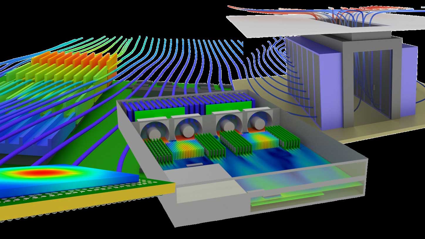
For thermal analysis modeling methods, seeThe Importance of Thermal Analysis and Modeling in PCB Design; For the aluminum substrate solution, seeHigh-Efficiency Heat Dissipation Solutions for Aluminum Substrates。
2. Improve the heat dissipation capacity of 5G circuit boards
Advanced: Four Preparations Before Getting Started with Layout
- List the heat sources: Sort by power consumption from highest to lowest, and identify the components that require priority attention;
- List of Thermosensitive Devices: Crystal oscillators, sensors, precision reference sources, electrolytic capacitors, etc.—specify their maximum operating temperature;
- Draw the direction of the airflow: Identify the air inlets, air outlets, and duct routing, and mark the upstream and downstream directions;
- Define Structural Constraints: The location of the chassis cooling vents, height-restricted areas, screws, and mounting points—these factors determine where components can be placed.
Once you’ve completed these four steps, component placement will shift from being “based on experience” to being “based on constraints.” In particular, step 3 is often overlooked: the optimal layout for the same board under natural convection and forced air cooling is completely different,Start by drawing the ductwork; that will provide a basis for the layout.。

For component placement rules, see13 Rules for Laying Out Components on Printed Circuit Boards; For information on wiring reliability, seeDFM Reliability Design for PCB Routing。
a. Heat-sensitive components are placed in the cool air zone
Place heat-sensitive components in areas of the device where cool air circulates well to ensure they are not affected by high temperatures.
b. The temperature sensor is placed in the hottest location
Place the temperature sensor in the location within the equipment that is most susceptible to heat, so that temperature changes can be monitored in a timely manner.
c. Arrange components in a logical layout
Arrange the components on the same printed circuit board in zones based on their heat generation and heat dissipation capabilities. Place components that generate little heat or have low heat resistance at the very beginning (inlet) of the cooling airflow, and place components that generate a lot of heat or have high heat resistance at the very end of the cooling airflow.
d. Optimize horizontal and vertical layouts
Horizontally, high-power devices should be placed close to the edges of the printed circuit board to shorten the heat transfer path. Vertically, high-power devices should be placed as close as possible to the top of the printed circuit board to minimize the impact of their operating temperatures on other components.
e. Study airflow paths
Consider the airflow path to ensure that air can flow smoothly through the heat-dissipation area. Avoid leaving large open spaces on the printed circuit board to make the most of the airflow.
f. Place temperature-sensitive components in the area with the lowest temperature
Place temperature-sensitive components at the bottom of the device or in a cooler location to minimize the likelihood that they will be affected by heat-generating components.
g. Place the components with the highest power consumption
Place the components with the highest power consumption and greatest heat generation near the areas with the best heat dissipation to ensure that heat is dissipated promptly.
Advanced: Board-Level Cooling Methods Ranked by Cost-Effectiveness
- Optimize the Layout: Zero cost often yields the most significant results, so this should be prioritized;
- Copper Foil Lamination and Copper Cladding: Minimal increase in costs, improved horizontal diffusion;
- Heat Dissipation Via Array: Create a vertical passage; this is low-cost, but be mindful of the effects of welding;
- Rear window with exposed copper and heat sink: The results are noticeable, but this requires a balance between structure and cost;
- Heavy-gauge copper foil or thick copper plate: Improves both current-carrying capacity and heat dissipation, with moderate costs;
- Metal Substrate: The shortest heat transfer path; high cost and typically single-sided;
- Embedded Copper Blocks: For localized hotspots, this is the most expensive option.
We recommend evaluating the process in this order and stopping at whichever step meets the requirements. For many projects, the issue is resolved as early as the first or second step, so there is no need to proceed directly to the metal substrate.
- Quantify First, Then Choose a Solution: Estimate the heat flux density, then compare it with the performance ranges of each method;
- Don't rely solely on one approach: The combined effect of layout, copper foil, and vias is usually better than doubling the investment in any single method;
- Provide a means of verification: Place temperature sensors near the hottest spots; only after mass production can we confirm whether the design meets the requirements.

For information on thermal lag, seeThermal Hysteresis Issues in PCB Design; For information on the stability of multilayer boards, seeStability and Reliability of Multilayer PCBs。
3. Conclusion
Heat dissipation in 5G circuit boards is a key factor in ensuring device performance and reliability. Through proper layout and design, the heat dissipation capacity of 5G circuit boards can be enhanced, ensuring stable device operation in high-temperature environments. Jingpeng Electronics recommends paying close attention to heat dissipation requirements during the design process of 5G circuit boards to meet growing market demand.
Advanced: Thermal Design Verification and Three Common Misconceptions
- Misconception 1: Focusing Only on the Average Temperature: What truly determines reliability is the temperature at the hottest junction; the average temperature can mask localized overheating;
- Misconception 2: Focusing Only on Steady State: Since 5G devices typically operate in bursts, transient temperature rises and thermal shocks are equally critical;
- Misconception 3: Treating Heat Sinks as a Universal Solution: If the thermal resistance between the heat source and the heat sink is very high, even the largest heat sink will have limited effectiveness.
We recommend doing three things during the verification process:Identifying hotspots through thermal simulation, calibrating the model based on measurements from the first prototype, and retesting under extreme operating conditions. The third item is the one most likely to be omitted, but the actual load of 5G equipment fluctuates significantly. If operating conditions involving prolonged full-power operation have not been tested, the likelihood of on-site issues will increase significantly.
In addition, attention should be paid to the interaction between thermal management measures and RF performance: large copper planes and metal heat sinks can alter the electromagnetic environment near the antenna; once the thermal design is complete, it is important to verify that the RF performance has not deteriorated.
Frequently Asked Questions
1. Why is heat dissipation so important for 5G circuit boards?
- 5G devices typically generate a significant amount of heat, and effective heat dissipation ensures their performance and stability.
2. What methods can be used to improve the heat dissipation capabilities of 5G circuit boards?
- Heat dissipation capabilities can be improved through methods such as proper component layout, zoning, and airflow path analysis.
3. Why should heat-sensitive components be placed in the cool air zone?
- This ensures that heat-sensitive components are not affected by high temperatures, thereby maintaining their accuracy.
4. Why should the temperature sensor be placed in the hottest location?
- Temperature sensors should be placed in locations most susceptible to heat so that temperature changes can be monitored in a timely manner.
5. Why should components that generate a lot of heat be placed near the edges of the printed circuit board?
- This can shorten the heat transfer path and improve heat dissipation efficiency.
6. Do heat-dissipating vias affect RF performance?
It is possible. Dense via arrays can alter the local electromagnetic environment, which is particularly sensitive near RF traces. The solution is to route heat-dissipating vias away from RF-sensitive areas or to maintain sufficient spacing between the RF area and the heat-dissipating area; if necessary, use simulation to verify that the impact is manageable.
7. What are the unique aspects of thermal design for outdoor 5G equipment?
It is necessary to consider both the additional heat load caused by solar radiation and the heat dissipation limitations of a fully sealed structure. A common approach is to rely on the outer wall of the enclosure for heat dissipation; therefore, the enclosure material, color, and fin design are all directly related to thermal performance. Internally, heat must be efficiently conducted to the enclosure walls.
8. Why does the area around the power amplifier require special treatment?
The power amplifier is the component with the highest thermal flux density on the board, and its efficiency directly determines the board’s total thermal load. In addition to providing heat sink pads and via arrays beneath the component, care must be taken to thermally isolate the power amplifier from adjacent components to prevent sensitive components from overheating beyond their specifications.
9. Should thermal design take low-temperature operating conditions into account?
Yes. During cold starts, the parameters of some components differ significantly from those at high temperatures, particularly crystal oscillators and electrolytic capacitors. In addition, repeated temperature cycling can cause solder joint fatigue; therefore, thermal design must not only prevent overheating but also take into account the magnitude and rate of temperature changes.
10. How does plate thickness affect heat dissipation?
The thicker the board, the greater the longitudinal thermal resistance, making it more difficult for heat to transfer from the top layer to the bottom layer; however, thicker boards also have greater thermal capacity, resulting in a more gradual transient temperature rise. Therefore, thicker boards are better suited for use with heat-dissipating via arrays, while thinner boards rely more on lateral copper routing to distribute heat.
11. Can standard FR-4 be used for 5G boards?
Consider the operating frequency. In some Sub-6GHz applications, low-loss FR-4 can be used, while the millimeter-wave band typically requires specialized high-frequency materials. In terms of heat dissipation, FR-4’s poor thermal conductivity is a weakness; areas with high heat flux density must be addressed using copper foil, vias, or metal substrates.
Related Reading:13 Rules for Laying Out Components on Printed Circuit Boards · Stability and Reliability of Multilayer PCBs
