

ENIG (Electroless Nickel Immersion Gold) is a surface treatment process widely used in PCB manufacturing. This article will provide an in-depth exploration of the ENIG process, including its advantages, disadvantages, and detailed process steps.
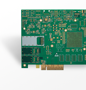
1. Overview of the ENIG Process
The ENIG process, commonly known as electroless nickel-immersed gold plating or electroless gold plating, is used for the surface treatment of printed circuit boards. It is widely used on PCBA boards inside mobile phones and on some BGA carrier boards.
Compared to traditional nickel-gold plating processes, the ENIG process is simpler to manufacture; it does not require applying an electric current to the circuit board or routing wires to each pad to be plated, making the process more efficient and relatively less expensive.
2. Advantages of ENIG
2.1 Simple Process
The ENIG process does not require complex electroplating equipment or current control, so it is relatively simple and easy to implement. This also helps improve manufacturing efficiency.
2.2 Suitable for Complex PCB Designs
The ENIG process is suitable for complex PCB designs, including those with high-density pads and fine-pitch pads. It provides a reliable surface finish for these complex designs.
2.3 Preventing Oxidation
The gold layer in the ENIG process effectively prevents oxidation of the nickel layer, thereby improving soldering reliability.
3. Disadvantages of ENIG
3.1 Low Weld Strength
Compared to some other surface treatment processes, ENIG may have lower solder joint strength. This could be a problem in certain applications.
3.2 The "Black Pad" Issue
The ENIG process can sometimes cause "black pad" issues, a type of soldering defect that may affect soldering quality.
4. Detailed Steps of the ENIG Process
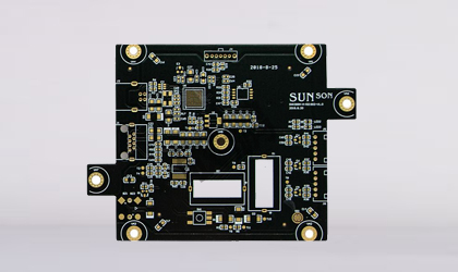
The following are the detailed steps of the ENIG process:
4.1 Pretreatment
The purpose of pretreatment is to remove oxides from the copper surface and roughen it to improve the adhesion of the subsequent nickel and gold layers.
4.2 Micro-erosion
The micro-etching step uses sodium persulfate or sulfuric acid to remove the oxide layer from the copper surface and reduce the depth of the scratches caused by brushing during pretreatment. Excessively deep scratches often lead to problems with gold plating attacking the nickel layer.
4.3 Activation
The activation step involves coating the copper surface with a layer of palladium (Pd) to serve as a catalyst for electroless nickel plating. This is because the copper surface cannot directly initiate the electroless nickel plating reaction; palladium is required as a catalyst.
4.4 Chemical Nickel
The primary function of chemical nickel (Ni/P) is to prevent migration and diffusion between copper and gold, and to react chemically with tin during the subsequent soldering process to form an intermetallic compound (IMC).
4.5 Immersion Gold Plating
The primary purpose of immersion gold plating is to protect the nickel layer and prevent it from oxidizing. Gold does not participate in chemical reactions during the welding process, but it must be thick enough to cover the nickel layer in order to prevent oxidation.
5. Conclusion
The ENIG process is relatively simple, cost-effective, and suitable for complex PCB designs. However, it also has some drawbacks, such as low solder joint strength and the potential for black pad issues. Therefore, when selecting a surface treatment process, it is necessary to weigh the pros and cons and make a choice based on specific application requirements.
Frequently Asked Questions
1. What are the main advantages of the ENIG process?
The main advantages of the ENIG process include its simplicity, suitability for complex PCB designs, and protection against oxidation.
2. What are the disadvantages of the ENIG process?
The main drawbacks of the ENIG process include low solder strength and the potential for black pad issues.
3. What is the "black pad" issue?
The "black pad" issue refers to a soldering defect that may result from the ENIG process and can affect soldering quality.
4. What is the difference between the ENIG process and the nickel-gold plating process?
The ENIG process does not require power to be applied to the circuit board, nor does it require wiring to be routed to each pad to be plated, making it simpler and more efficient than the nickel-gold plating process.
5. For which PCB designs is the ENIG process suitable?
The ENIG process is suitable for complex PCB designs, including high-density pads and fine-pitch pads.
