

The PCB industry—short for printed circuit board—may be a relatively unfamiliar field to many people. It involves numerous technical terms and concepts that perhaps only industry experts can fully understand. In this article, we’ll answer eight classic questions about the PCB industry to help you better understand this field.
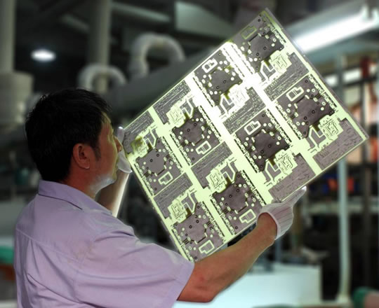
1. What is a PCB?
PCB 即Printed Circuit Board, which translates to Chinese asPrinted Circuit Board. It is a board on which interconnections and printed components are formed on a common substrate according to a predetermined design. PCBs can be classified into rigid printed circuit boards, flexible printed circuit boards, and rigid-flex printed circuit boards based on the type of substrate. They can also be classified into single-sided, double-sided, and multilayer printed circuit boards based on the number of layers containing the conductor patterns.
When combined, these two classification dimensions form the complete PCB product matrix:
| By Substrate | By Number of Floors | Featured Products | Mainstream Applications |
|---|---|---|---|
| Rigid Printed Circuit Board (Rigid PCB) | Single-sided board | Single-sided paper-based, CEM-1, FR-4 single-sided | Home Appliance Control Boards, LED Light Boards |
| Rigid Printed Circuit Board | Double-sided board | FR-4 Double-Sided, Metal-Clad Board | Power Supply Boards, Industrial Control, Lighting |
| Rigid Printed Circuit Board | Multilayer Board | 4–20-layer FR-4, HDI, and IC carrier boards | Servers, communications equipment, cell phone motherboards |
| Flexible Printed Circuit (FPC) | Single/Double/Multi-layer | PI Substrate FPC | Foldable screens, camera modules, wearable devices |
| Rigid-Flex Printed Circuit Boards | Floors 4–12 (including the rigid zone) | Rigid-Flex Board | In-Vehicle Modules, Aerospace, Healthcare |
There's also another button to pressSpecial FeaturesThis classification determines both the quotation and the manufacturing process: high-frequency boards, thick-copper boards, metal-core boards (aluminum-core/copper-core), ceramic boards, HDI (High-Density Interconnect), IC carrier boards, and boards with embedded components. Within this classification, each category has entirely different manufacturing processes and unit prices. For the specific process windows of each category, seePCB Manufacturing Capabilities。
2. What does PE stand for?
PE 即Product Engineering Department, which translates to Chinese asProduct Engineering Department. The department's primary functions include pre-production data processing, tooling, and sample tracking. It consists of three functional teams: MI (Manufacturing Institute), CAD/CAM, and Sample.
PE is the most critical department in a PCB factory. When customers send Gerber files and drawings, the first stop is PE: they determine whether the design is feasible, how to implement it, and where the risks lie, and then generate the manufacturing instructions (MI) to be handed over to the production line.Eighty percent of a panel factory’s engineering capabilities are reflected in the PE team.—With the same equipment, a factory with strong PE capabilities can achieve a yield rate of 98%, while a factory with weaker capabilities may only reach 90%.
Let’s take a closer look at the three functions of PE:
- Data Processing: Gerber analysis, stackup design, impedance calculation, panelization, and design of process margins and registration holes.
- Tool Making: Molds, drill strips, routing strips, test fixtures, stencils, carriers.
- Sample Follow-Up: First-article approval, issue reporting, and parameter finalization—converting the findings from pilot production into mass production standards.
3. What is CAD/CAM?
CAD/CAM 即Computer-Aided Design/Computer-Aided Manufacturing, which translates to Chinese asComputer-Aided Design/Computer-Aided Manufacturing. It is a technology that uses computers to assist in product design and manufacturing.
In the context of PCB design, the division of labor between CAD and CAM is very clear:CAD is used for design(Generate schematics and layouts using EDA tools such as Altium Designer, Allegro, KiCad, PADS, etc.),CAM is the manufacturing end(Engineering software such as Genesis, InCAM, and UCAM is used at PCB manufacturers to convert customer data into production-ready tool files.)
What a CAM engineer needs to do after receiving Gerber files is far more complex than simply ”opening them to take a look”:
- Data Completeness Check: Check whether all layers are present and whether the layer definitions match the design.
- DFM Analysis: Do the line width and spacing, hole diameter and spacing, solder mask bridges, and annular ring width meet process capability requirements?
- Compensation and Correction: Compensate for line width based on the etching factor, compensate for layer misalignment based on lamination data, and compensate for drill hole diameter.
- Page Layout and Typesetting: Panel layout, process margins, optical alignment marks, test points, V-cuts, and stamp holes.
- Output Tool Files: Photomounting files, drill tapes, routing tapes, AOI programs, and electrical testing programs.
When submitting CAD designs to a PCB manufacturer, the following information must be included along with the Gerber files; otherwise, the CAM system will have to guess:
- Definition of Levels and Hierarchy: Which layer is the top layer, bottom layer, or inner layer, and what is the order?
- Finished Plate Thickness and Tolerances: Any specific requirements (card insertion, crimping, housing) must be clearly stated.
- Impedance Requirements: Target values, tolerances, reference layers, and differential pairs.
- Surface Treatment and Solder Mask/Character Color。
- Acceptance Criteria: Is it IPC-6012 Class 2 or Class 3? Are there any special inspection items?
- IPC-356 Network Diagram: Used for electrical calibration; without it, open-circuit and short-circuit verification cannot be performed.
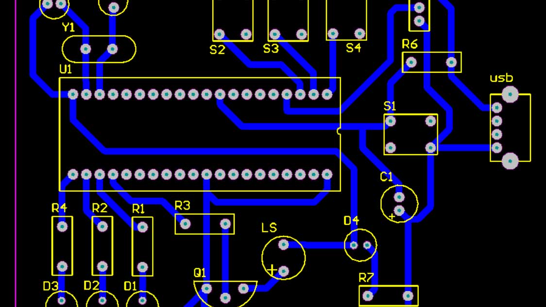
For a complete CAM workflow, please refer toThe 9 Basic Steps of CAM Production. Every adjustment made during the CAM process ultimately affects the yield of the finished product, which is why most rework during the prototyping phase occurs at this stage.
4. What is MI?
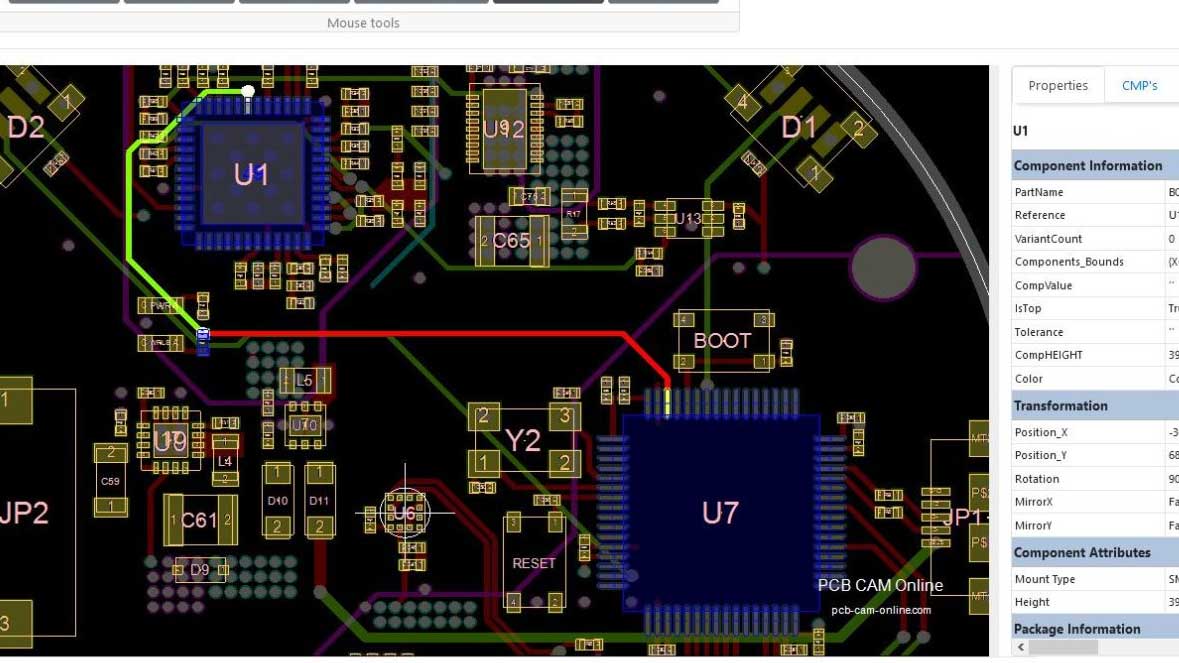
MI 即Manufacturing Institute (or Instruction), which translates to Chinese asPre-Production Preparation and Process Instructions. This serves as an important guide for preparing and planning the production process prior to manufacturing.
A complete MI typically consists of more than a dozen items and serves as the sole basis for operations on the production line:Board Model and Thickness, Copper Thickness, Stack-Up and Layer Sequence, Finished Board Thickness and Tolerances, Impedance Requirements, Minimum Line Width and Spacing, Via Diameter and Tolerances, Surface Finish, Solder Mask and Marking Colors, Outline and Forming Method, Acceptance Criteria (IPC Grade), Special Process Requirements, Packaging Method。
The three issues in MI that are most likely to cause problems and are the most common sources of disputes between buyers and sellers:
- Acceptance Criteria: Whether to specify ”IPC-6012 Class 2” or “Class 3” has a significant impact on cost and the criteria for determination; this must be clearly stated in the MI.
- Impedance Requirements: Target value, tolerance, test strip position, and reference layer—if any one of these is missing, verification is not possible.
- Sheet Thickness Tolerance: Default ±10%; if there are fit requirements (such as card insertion or crimping), stricter tolerances must be specified.
5. What is a paradigm?
Paradigm It is an **ERP (Enterprise Resource Planning)** system developed by Cimnet Systems Inc. of the United States, primarily used in the PCB and related industries. At the core of ERP is the enterprise resource management system, which integrates resources across enterprise management, business processes, master data, human and material resources, and computer hardware and software.
The PCB industry needs specialized industry ERP because general-purpose ERP systems cannot handle two key aspects:Dynamic Conversion for Page Layout(How many sets fit on a large sheet of material, how many pieces are in each set, and how to allocate the scrap rate) andProcess-Level Cost Allocation(A single panel goes through 30–50 production steps, and the labor hours and materials for each step must be traceable.)
Modern panel factories typically consist of a three-layer system stacked on top of each other:ERP Manage orders and finances,MES Manage workflow and data collection,APS Manages production scheduling. Paradigm is part of the first layer. Only after all three layers are integrated can customers track ”which production stage this batch of boards is currently in and which batch of substrates was used”—this system is what enables the batch traceability required by automotive and medical customers.
6. What is APQP?
APQP 即Procedure for Advanced Product Quality Planning and Control, which translates to Chinese asProcedures for Pre-Production Product Planning and Control. It is a process and method used to plan and control product quality.
7. What is PPAP?
PPAP 即Production Part Approval Process Procedure, which translates to Chinese asProduct Approval Process. It is primarily used in automotive products to ensure that manufactured parts meet quality standards.
APQP and PPAP are two interconnected processes:APQP is a process(The process from project initiation to mass production consists of five stages, with quality planning carried out early on),PPAP is a deliverable(A set of documentation submitted prior to mass production to demonstrate that ”I can consistently produce conforming parts.”) PPAP is classified into five levels based on the strictness of the requirements:
| Level | Submit Content | Applicable Scenarios | Typical Document Volume |
|---|---|---|---|
| Level 1 | Statement of Guarantee (PSW) | Low risk; long-standing supplier relationship | 1–2 servings |
| Level 2 | PSW + Sample + Some Supporting Data | Regular Suppliers | 5–10 servings |
| Level 3 | PSW + Sample + Complete Supporting Data | Default Grades for Automotive Parts | 15–20 servings |
| Level 4 | Level 3 + Special Requirements (as specified by the customer) | Safety Components, Critical Components | 20+ copies |
| Level 5 | Level 3 + On-site Evaluation | New Suppliers, Significant Changes | 现场审核 |
PPAP Level 3 里与 PCB 直接相关的文件通常包括:尺寸检验报告、材料与性能试验报告(含阻燃等级、 peel strength、热应力)、过程能力研究(CPK)、控制计划、过程流程图、FMEA、以及全尺寸全性能的全检记录。这套文件的准备周期一般是 4–8 周,是车载项目周期里最容易被低估的一段。车载板与常规板的差异可参考Key Differences Between Automotive Circuit Boards and Conventional Circuit Boards。
8. Gerber是什么?
Gerber 是一种格式,它是由线路板设计人员使用专业的电子设计自动化(EDA)或者PCB CAD软件输出的。这种格式通常用于制作光刻胶板,是电子行业的公认标准格式之一。
Gerber 本质上是一种二维矢量描述格式,用”画”或”闪”两种动作来描述图形。目前主流是 RS-274X(扩展 Gerber),它把光圈表(Aperture)内嵌在文件里,避免了老式 RS-274D 需要单独附带光圈表的麻烦。近年兴起的 Gerber X2 与 ODB++ 则进一步把层别属性、阻抗要求、孔属性等元数据一起打包,减少 CAM 端的猜测。
一套完整的 Gerber 交付包应该包含:
| 文件类型 | 常规扩展名 | 作用 | 缺失后果 |
|---|---|---|---|
| 线路层 | .GTL / .GBL / .G1… | 外层与内层导体图形 | 无法生产 |
| Solder Mask | .GTS / .GBS | 阻焊开窗 | 全板覆盖或全板开窗 |
| 字符层 | .GTO / .GBO | 丝印标识 | 无字符 |
| 锡膏层 | .GTP / .GBP | 钢网开口(SMT 用) | 钢网无法制作 |
| 钻孔文件 | .TXT / .DRL | 孔位与孔径 | 无法钻孔 |
| 外形/锣带 | .GKO / .GM1 | 板外形与槽孔 | 外形不确定 |
| IPC-356 Network Diagram | .IPC | 用于电测比对 | 无法做开短路验证 |
关于 Gerber 与 ODB++ 的互转,可以参考How to Generate PCB Files from GERBER/ODB++ Files。
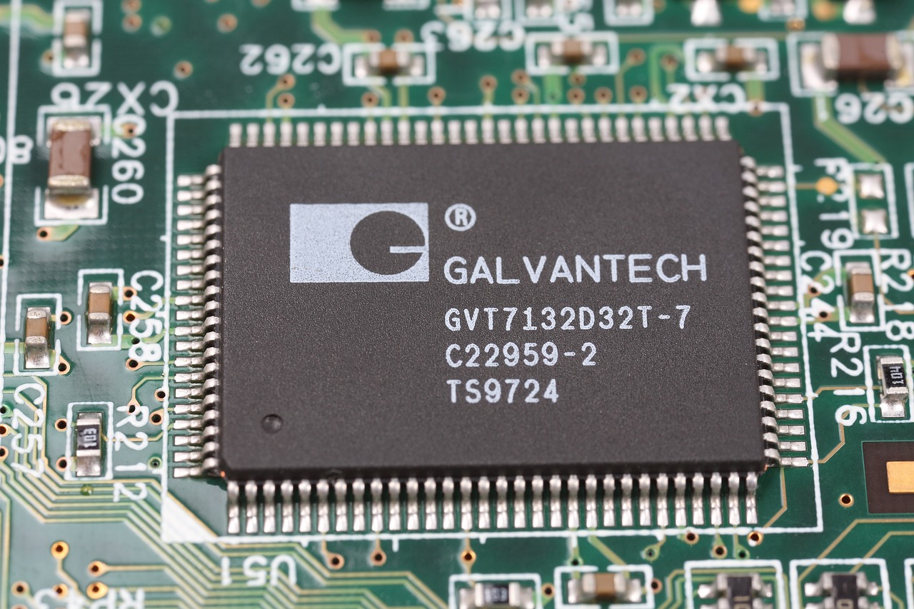
通过了解这些经典问题的答案,您可以更好地理解PCB行业的基本概念和术语。如果您对PCB行业或相关领域有更多疑问,欢迎联系我们以获取更多信息。
9. 板厂工程资料的完整流转
把上面这些术语串起来,就是一份订单从下单到出货的完整链路:
- 客户下单:提交 Gerber + 图纸 + 工艺要求(板厚、铜厚、表面处理、阻抗、验收标准)。
- 工程评审(PE):CAM 工程师做 DFM 分析,输出问题清单与工程建议(EQ)。
- 客户确认:回复 EQ,确认补偿方案或改版。
- 出 MI:把确认后的方案写进 MI,作为产线唯一作业依据。
- Tool Making:光绘、钻带、锣带、模具、测试架、钢网。
- 计划排产(ERP/APS):开料计划、工序排程、交期承诺。
- 量产(MES):工序流转、参数采集、SPC 监控。
- 出货:电测报告、切片报告、阻抗报告、出货检验报告、包装与追溯标签。
10. 另外 10 个高频术语
除了上面 8 个,日常沟通里还会反复出现这些词,一并解释清楚:
- EQ(Engineering Query):工程询问单,板厂就资料问题向客户提问的正式文件,回复速度直接决定交期。
- Panel / Set / Pcs:拼版 / 单元 / 单个成品。报价与产能统计的单位,三者换算关系要问清楚。
- Annular Ring:孔环,焊盘外缘到孔壁的导体宽度,太小会在对位偏差下破盘。
- Aspect Ratio:厚径比,板厚与最小孔径之比,超过 8:1 电镀难度显著上升。
- V-CUT / 邮票孔:分板方式,V-CUT 适合直线分板,邮票孔适合异形。
- Flying Probe / Fixture Test:飞针测试 / 测试架测试,前者适合小批量,后者适合大批量。
- CAF:导电性阳极丝,湿度与电场作用下沿玻纤生长的离子迁移,是绝缘失效的常见原因。
- Solder Mask Dam:阻焊桥,细间距焊盘之间必须保留的阻焊条。
- Tg / Td:玻璃化转变温度 / 分解温度,决定板材耐温等级。
- ICT / FCT:在线测试 / 功能测试,PCBA 阶段的两种测试方式。

Frequently Asked Questions (FAQs)
1. PCB行业有哪些常见的应用领域?
PCB行业广泛应用于电子、通信、汽车、医疗设备等领域,用于制造各种电子设备的核心组件。
2. PCB的制造过程包括哪些关键步骤?
PCB制造包括设计、印刷、切割、钻孔、电镀、阻焊、测试等多个关键步骤。
3. 为什么PCB的设计和制造如此重要?
PCB的设计和制造质量直接影响到电子产品的性能和可靠性,因此非常重要。
4. PCB制造中有哪些常见的质量控制方法?
常见的质量控制方法包括MI(制造前准备及流程制作指示)、APQP(生产前产品制品规划和控制计划程序)和PPAP(生产产品认可程序)等。
5. 如何选择适合自己需求的PCB制造厂家?
选择PCB制造厂家时应考虑其经验、技术能力、质量控制体系以及交货时间等因素,以确保满足自己的需求。
6. APQP 和 PPAP 是一回事吗?
不是。APQP 是过程,从立项到量产分五个阶段,把质量策划做在前面;PPAP 是交付物,在量产前提交的一套证明文件。可以理解为”APQP 是做质量策划的方法论,PPAP 是这个方法论结束时交出的作业”。
7. 为什么板厂总催着回复 EQ?
因为 EQ(工程询问单)不确认,CAM 就无法出 MI,后续的工具制作、排产、备料全部卡住。EQ 的回复速度是决定交期的第一变量,很多”交期延误”实质上是 EQ 在客户侧停留了几天。
8. 发 Gerber 还是 ODB++ 更好?
ODB++ 更好。它把层别属性、阻抗要求、孔属性等元数据一起打包,CAM 端不用猜层别定义,出错概率低。但目前仍有不少板厂只支持 Gerber,实际做法是发 RS-274X 完整包(含 IPC-356 网表),并附一份层别说明与工艺要求书。
9. 为什么同一份 Gerber 两家板厂报价差很多?
因为 MI 里没写死的项目,各家按自己的默认工艺理解:验收标准(Class 2 还是 Class 3)、板厚公差、阻抗公差、表面处理品牌、是否全检、是否含阻抗报告,这些都会显著改变成本。报价前把 MI 要素写清楚,价差会立刻收敛。
10. 小批量打样和大批量量产,工程流程有什么不同?
打样阶段 PE 会做首件确认与参数固化,出问题多靠人工判断;量产后这些参数被写进 MI 与 SPC 控制计划,转为自动监控。车载与医疗项目还要求在打样阶段就同步启动 APQP,避免量产时才补 PPAP 文件。
通过这些问题和答案,您可以更好地理解PCB行业,并为相关决策提供有用的信息。如果您需要更多详细信息,请随时联系我们,我们将竭诚为您提供帮助。
Further Reading:电路板厂常用专业词汇中英文对照
