

During the PCB manufacturing process, AOI (Automated Optical Inspection) is typically performed twice: once after the inner layer traces are completed, and again after the outer layer traces are completed.
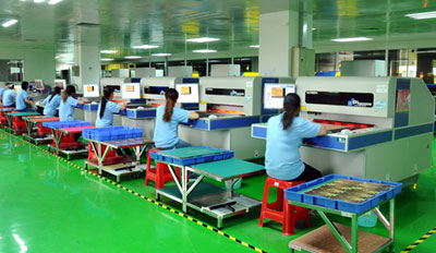
What is AOI?
AOI stands for Automated Optical Inspection, an advanced automated inspection technology designed to ensure the quality and reliability of PCBs. The basic principle of this technology is to compare a reference image with an image of the actual manufactured PCB. The reference image is typically derived from CAM (Computer-Aided Manufacturing) data, while the image of the actual PCB is obtained by scanning the board using optical components.
Why are two AOI inspections necessary?
In the PCB manufacturing process, the production of inner-layer and outer-layer circuits involves different requirements and processes. Therefore, to ensure quality at every stage, AOI inspections are typically conducted at two key stages.
First AOI after inner-layer trace fabrication
The first AOI inspection is typically performed after the inner layers have been fabricated. This stage involves the internal structure of the PCB, including the connections between layers and the insulation layers. The AOI system scans the PCB to check for short circuits, open circuits, or other anomalies between conductors. This helps ensure the quality and reliability of the inner layers.
Second AOI after completion of the outer layer traces
The second AOI inspection is conducted after the outer layer traces have been completed. The outer layer typically includes the PCB’s final layout, which comprises elements such as the pads connected to components. The AOI inspection at this stage focuses primarily on the quality of pad connections, the correct placement of components, and any defects on the PCB surface. Through the second AOI, manufacturers can ensure that the final PCB meets standards for performance and reliability.
The importance of AOI in PCB manufacturing is self-evident. It helps detect and correct potential issues, ensuring that the final PCB products meet quality standards. This not only helps reduce errors and scrap rates during the manufacturing process but also improves the performance and reliability of PCBs in practical applications.
Although AOI may increase manufacturing costs and lead times, its critical role in PCB manufacturing is irreplaceable. It provides manufacturers with an effective means of quality control, ensuring that the final PCB products meet customer requirements and perform well in a variety of applications.
Frequently Asked Questions
1. What is AOI?
AOI stands for Automated Optical Inspection, a type of automated inspection technology used to check the quality and reliability of PCBs.
2. Why are two AOI inspections necessary?
AOI is typically performed twice because the manufacturing requirements and processes for inner-layer and outer-layer circuits differ. Conducting inspections in stages helps ensure quality at every stage.
3. How does AOI work?
AOI systems inspect for potential issues—such as pad connection quality, component placement, and defects—by comparing reference images with images of the actual manufactured PCBs.
4. Why is AOI important in PCB manufacturing?
AOI can help detect and correct issues, ensuring that PCB products meet quality standards, thereby reducing manufacturing errors and improving performance reliability.
5. Does AOI increase manufacturing costs?
Yes, AOI may increase manufacturing costs and lead time, but it provides manufacturers with an effective means of quality control that helps improve the quality of the final product.
