

In PCB (Printed Circuit Board) design, the solder mask and paste mask are the core layers that ensure soldering reliability and circuit performance.
Beginners often confuse the functions of the two, while experienced designers need to have a deep understanding of their material properties, process compatibility, and parameter design logic—this article will move from basic definitions to advanced applications, providing a comprehensive analysis of the technical points and practical value at both levels.
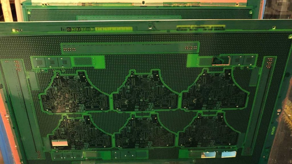
Solder Mask: From Coating to Performance Barrier
Definitions and the Nature of Materials
The solder mask is not simply an “insulating coating,” but rather a functional film made from photosensitive epoxy resin ink (the most common type) or thermosetting resin. It is typically green (accounting for over 80%), but can also be customized to blue, red, black, and other colors as needed. Its core characteristics must meet three key requirements:
Electrical Insulation Properties: Volume resistivity ≥ 10¹⁴ Ω·cm (at 25°C), breakdown voltage ≥ 20 kV/mm; prevent short circuits between adjacent conductors;
Environmental Stability: Withstands thermal cycling from –40°C to 125°C (industrial-grade standard); resists moisture penetration (water absorption rate ≤ 0.51 TP3T/24h at 85°C); and resists chemical corrosion (e.g., flux residues, cleaning agents);
Process Compatibility: Can be formed via photolithography or screen printing; adhesion to PCB substrates (FR-4, aluminum substrates, etc.) is ≥5 N/cm (based on peel strength test standards).
Technical Details of Core Features
Welding Control: Precise Design of Solder Mask Openings
The solder mask enables solder placement through “window openings” (which expose the pad areas); the dimensions of these openings must strictly adhere to the **“pad + extension” rule"**:
Standard SMD pads: The window size is 0.1–0.2 mm larger than the pad (with a 0.05–0.1 mm extension on each side). This prevents solder mask from covering the pad and causing cold solder joints, while also preventing adjacent pads from bridging due to an excessively large window;
High-frequency signal pads: The window extension should be reduced to 0.03–0.05 mm to minimize reflection interference from the solder mask edge (especially at frequencies above 1 GHz);
Power Device Pads: When using wave soldering, an additional 0.1 mm of “overflow space” must be reserved around the openings to prevent solder buildup, which can lead to poor heat dissipation.
Electrical Isolation: Optimization for Different Scenarios
High-density PCBs (line width ≤ 0.1 mm): The solder mask must be capable of covering fine circuits, with solder mask bridges (the solder mask area between two conductors) having a width of ≥ 0.08 mm to prevent short circuits caused by solder mask bridge fractures during the manufacturing process;
High-voltage PCBs (voltage ≥ 1 kV): The solder mask thickness must be increased to 30–50 μm (typically 10–20 μm), and a “double-layer solder mask” process must be used to enhance breakdown resistance.
Substrate Protection: The Key to Extending PCB Lifespan
The solder mask isolates the copper foil from oxygen, moisture, and dust in the air, slowing down the rate of oxidation—uncovered copper foil is prone to forming an oxide layer (CuO/Cu₂O) at room temperature, which reduces the solderability of the pads; In contrast, copper foil covered with a solder mask can extend its solderability shelf life from 3 months to over 12 months (in compliance with the IPC-J-STD-003 standard).
Type and Process Matching
The solder mask is divided into a top layer (Top Solder) and a bottom layer (Bottom Solder), but the appropriate type must be selected based on the manufacturing process:
Light-Patterned Solder Mask (LPI):
Suitable for fine-line PCBs (line width/spacing ≤ 0.1 mm), with a resolution of up to 0.05 mm; precise windowing is achieved through UV exposure and development;
Screen-Printed Solder Mask:
Suitable for standard PCBs (line width ≥ 0.15 mm), this method is cost-effective but has limited resolution (minimum aperture ≥ 0.2 mm). Care must be taken when selecting the screen mesh count (typically 300–400 mesh; the higher the mesh count, the more uniform the coating).
Paste Mask (Solder Paste Layer)
Definition of "Paste Mask"
Paste Mask, known in Chinese asSolder Paste Layer... is a special layer applied to a PCB. It is typically used for soldering surface-mount (SMD) components. The solder paste layer contains holes that correspond to the solder joints of the SMD devices on the circuit board.
Functions of the Solder Paste Layer
The primary function of the solder paste layer is to ensure precise placement of solder joints for SMD components. Specifically, the solder paste layer serves the following purposes:
Making a Solder Stencil:
During the soldering process for surface-mount devices (SMDs), a layer of solder paste is used to create steel stencils (or steel sheets). The holes in these stencils correspond to the solder joint locations of the SMDs on the circuit board.
Controlling the Amount of Solder:
The design of the solder paste layer controls the amount of solder to ensure proper soldering. Too much or too little solder can lead to soldering quality issues.
Improving Welding Precision:
By using a layer of solder paste, solder can be applied more precisely to the solder pads of SMD components, thereby improving the accuracy and reliability of the soldering process.
Types of Solder Paste Layers
Solder paste layers are typically classified asTop Paste(top solder paste layer) andBottom Paste(bottom solder paste layer), used on the top and bottom of the circuit board, respectively. This accommodates different soldering requirements and component layouts.
In addition, the hole size in the solder paste layer is typically slightly smaller than the hole size of the actual solder joints on the circuit board; this can be fine-tuned by specifying expansion rules to ensure soldering accuracy and feasibility.
In PCB design, it is crucial to understand the roles of the solder mask and the paste mask. The solder mask is used to prevent unwanted soldering and provide electrical isolation, while the paste mask is used to control the placement of SMD component solder joints and improve soldering accuracy. Both layers play a critical role in PCB manufacturing and performance, so designers must clearly understand their functions and applications.
Different PCB manufacturing processes and software tools may use positive or negative notation to represent these layers, but these are merely different notations that do not affect the final manufacturing quality of the PCB.
In PCB design, it is also important to distinguish between the assembly layer and the trace layer, which are used to display the component outline and the actual physical layout, respectively. In addition, care must be taken when designing through-hole pads; the hole should be larger than the pin to facilitate soldering.
Finally, to ensure the success of your PCB design, it is essential to understand and master the concepts and applications of these key layers.
Industry Development Trends
Upgrades to Solder Mask Materials:
For automotive electronics (operating temperatures ranging from -40°C to 150°C), high-temperature-resistant solder mask inks (Tg ≥ 180°C) are gradually becoming more widespread; for flexible printed circuits (FPCs), bendable solder mask materials (elongation at break ≥ 50%) have become the mainstream choice.
Intelligent Solder Paste Coating:
When used in conjunction with AI-powered design software, the “optimal aperture size” can be automatically generated based on component packages (such as the “Paste Mask Expansion Wizard” feature in Altium Designer), thereby reducing human error.
Compatibility with Environmentally Friendly Processes:
The use of halogen-free solder mask ink (halogen content ≤ 900 ppm) in combination with lead-free solder paste is now a mandatory requirement. During the design process, the use of solder masks compatible with halogen-containing fluxes must be avoided to prevent solder joint failure caused by chemical reactions.
The design of the solder mask and solder paste layers is not merely about “defining areas,” but rather a systematic engineering process that involves “balancing performance, manufacturing processes, and cost.” From material selection to parameter fine-tuning, every step must take into account the PCB’s application scenarios (such as consumer electronics, industrial control, and automotive electronics) and manufacturing processes (such as reflow soldering and wave soldering)—only by thoroughly understanding the technical fundamentals can one design PCB products with high reliability and a long service life.
Frequently Asked Questions
Are the solder mask and solder paste layers necessary?
Yes, the solder mask and solder paste layers are typically essential in PCB design, as they are used for solder control and the accuracy of solder joint placement, respectively.
What is the purpose of the color of the solder paste layer?
Solder paste is typically green, blue, or red; the main purpose of these different colors is to distinguish between different PCB layers or to provide visual identification. The color itself does not affect functionality.
How can you ensure the accuracy of the solder mask and solder paste layers in PCB design?
In PCB design, specialized design software is typically used to create these layers. The design is then checked and verified by generating Gerber files to ensure that the dimensions and positions of the solder mask and solder paste layers are accurate.
What is the difference between the assembly layer and the printing layer?
The assembly layer is used to display the actual outline and nominal values of the components, while the silkscreen layer is used to display the component layout. The assembly layer is typically used for layout and assembly drawings, while the silkscreen layer is printed on the PCB.
Why should the aperture of the solder paste layer be slightly smaller than the solder joint?
The aperture of the solder paste layer is slightly smaller than the solder joint to control the amount of solder and ensure the accuracy and reliability of the solder joint. This can be fine-tuned using the expansion rule.
How does the thickness of the solder mask affect high-frequency signals?
In high-frequency PCBs (≥5 GHz), for every 10 μm increase in solder mask thickness, signal insertion loss increases by 0.1–0.2 dB/inch (due to an increase in dielectric loss, tanδ). Therefore, solder mask ink with a low dielectric constant (εr ≤ 3.5 @ 10 GHz) should be selected, and the thickness should be controlled between 10 and 15 μm.
Why is it necessary to adjust the aperture of the solder paste layer for lead-free solder paste?
The surface tension of lead-free solder is 30% to 50% higher than that of leaded solder, and it has poorer flow. If the same opening dimensions used for leaded solder are applied, “solder wetting failure” (where the solder joint forms a hemispherical shape rather than a crescent shape) is likely to occur. Therefore, the opening dimensions must be reduced to increase solder pressure and ensure proper wetting.
How to Fix Solder Mask Peeling?
Solder mask delamination is often caused by inadequate cleaning of the substrate (residual oil or oxide layers) or insufficient curing temperature (the standard curing temperature is 150°C for 30 minutes). During the design phase, “substrate pretreatment requirements” (such as chemical cleaning or micro-etching) must be specified in the Gerber files, along with the solder mask curing process parameters.
What are the key considerations for designing the solder paste layer for ultra-fine-pitch components (01005, 0.3 mm pitch QFP)?
A “laser-cut steel stencil + nano-coating” process must be used (to reduce solder adhesion). The dimensional tolerance of the solder paste apertures must be ≤±0.005 mm, and the edges of the apertures must be “rounded” (R ≥ 0.01 mm) to prevent stress concentration from causing deformation of the steel stencil.
