

High-layer-count printed circuit boards are typically defined as multilayer printed circuit boards with 10 or more layers, or even 20 or more layers.
Compared with traditional multilayer printed circuit boards, high-layer printed circuit boards are more difficult to manufacture and have higher requirements for quality and reliability.
It is primarily used in telecommunications equipment, high-end servers, medical electronics, aviation, industrial control, and military applications.
In recent years, with the rapid development of China’s telecommunications equipment market, the outlook for the high-layer printed circuit board market has been very promising.
Currently, the PCB manufacturers in China that mass-produce high-layer circuit boards are primarily foreign-owned companies or a very small number of domestically owned companies.
The manufacture of multilayer printed circuit boards requires not only advanced technology and equipment, but also the accumulated experience of technical and production staff. At the same time, the customer certification process for multilayer printed circuit boards is rigorous and complex.
Consequently, multilayer PCBs have a relatively high entry barrier and a long industrial production cycle. The average number of layers in multilayer PCBs has become an important technical indicator for measuring the technical capabilities and product portfolio of PCB manufacturers.
This article provides a brief overview of the main challenges faced in the manufacturing of multilayer printed circuit boards, as well as key control points for critical production processes, for your reference.
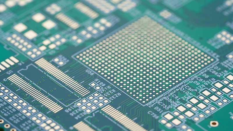
Major Manufacturing Challenges
Compared to conventional printed circuit boards, high-layer printed circuit boards have the following characteristics: thicker boards, more layers, denser traces and vias, larger cell sizes, and thinner dielectric layers. These characteristics result in the following manufacturing challenges:
1. Challenges in Interlayer Alignment
High-layer-count PCBs have numerous layers, and customers have increasingly stringent requirements for alignment between layers. Typically, the interlayer alignment tolerance is controlled to around ±75 μm. Controlling interlayer alignment becomes more challenging due to factors such as the large size of components on high-layer-count PCBs, fluctuations in ambient temperature and humidity, and inconsistent thermal expansion and contraction among different core layers.
2. Challenges in Manufacturing Inner-Layer Circuits
High-layer PCBs utilize special materials such as those with high TG, high-speed, high-frequency, thick copper, and thin dielectric layers, which place high demands on the fabrication of inner-layer traces and the control of pattern dimensions. This increases the difficulty of inner-layer trace fabrication. With narrower trace widths and spacing, issues such as open circuits, short circuits, and micro-short circuits become more frequent, leading to a lower yield rate. Dense circuits with multiple signal layers are prone to missed defects. The inner core layers are relatively thin and prone to wrinkling, leading to poor exposure. Most high-layer boards are used as system boards, featuring large component sizes and consequently high scrap costs.
3. Challenges in the Laminating Process
During the manufacturing process of high-layer-count printed circuit boards, stacking multiple inner-layer core boards and prepregs together can easily lead to defects such as board slippage, delamination, resin voids, and residual air bubbles. When designing the laminate structure, factors such as the material’s heat resistance, voltage withstand capability, resin fill ratio, and dielectric layer thickness must be taken into account. At the same time, it is necessary to establish a reasonable lamination process for high-layer boards. With a large number of layers, it is difficult to maintain consistency in thermal expansion control and dimensional coefficient compensation. Thin interlayer insulation layers can easily lead to failures in interlayer reliability testing.
4. Challenges in Drilling
Multi-layer PCBs use special materials with high TG, high-speed, high-frequency, and thick copper properties, which lead to increased drill hole roughness, burrs, and greater difficulty in removing drilling debris. The high number of layers results in increased total copper thickness and board thickness, making drill bit breakage more likely. The high density of BGAs results in narrow via wall spacing, which may lead to CAF failures. Increased board thickness also makes the board more prone to skewed drilling.
Key Control Points for Critical Production Processes
1. Material Selection
High-layer PCBs require electronic circuit materials with low dielectric constant and low dielectric loss, as well as low CTE, low water absorption, and high-performance copper-clad laminates. Different panel suppliers offer different series of inner-layer substrates. The choice of materials is critical to the fabrication and reliability of high-layer PCBs.
2. Design of Laminated Structures Under Compression
When designing laminated structures, factors such as the material’s heat resistance, voltage resistance, resin content, and dielectric layer thickness must be taken into account. The manufacturers of prepregs and core materials must be consistent. For panels with special high-TG requirements, appropriate materials must be selected.
3. Control of Interlayer Alignment
To control interlayer alignment, high-precision interlayer positioning methods must be used prior to lamination, such as four-slot positioning (Pin LAM) or a combination of hot melt and rivets. Establishing appropriate lamination process procedures and performing routine maintenance on the laminating press are key to ensuring lamination quality.
4. Inner Layer Circuit Process
In the manufacturing of high-layer-count printed circuit boards, laser direct imaging (LDI) systems can be incorporated to improve pattern resolution. High-precision alignment exposure systems can enhance pattern alignment accuracy and reduce alignment errors.
5. Laminating Process
Set up an appropriate pressing program, including control of the heating rate and temperature profile. Different sheet materials and prepregs require corresponding process parameters. Ensure adequate resin flow and curing while minimizing sheet slippage and interlaminar misalignment during the pressing process.
6. Drilling Process
Control the number of holes, feed rate, and rotational speed during drilling, and reduce them appropriately to minimize drill bit wear. For high-rise panels, it is necessary to accurately measure the panel’s expansion and contraction and use a suitable drilling machine for production.
Reliability Testing
Multi-layer printed circuit boards are typically used in system boards and must withstand high-temperature soldering tests. This requires a longer time through the reflow soldering process. Additionally, reliability testing is necessary to ensure the quality of the multi-layer printed circuit boards.
The manufacture of high-layer-count printed circuit boards is a field that demands a high level of technical expertise and experience. This article outlines the key control points for critical production processes, including material selection, stack-up design, interlayer alignment, inner-layer trace formation, lamination, and drilling.
We hope this information will serve as a reference and source of inspiration for our peers in the field of multilayer PCB manufacturing, and that it will promote the further development of technical research and exchange.
Frequently Asked Questions
1. How strict are the requirements for interlayer alignment in multilayer printed circuit boards?
Typically, the interlayer alignment tolerance for multilayer printed circuit boards is controlled to within approximately ±75 μm. This depends on the customer’s design requirements and the product’s application.
2. Why do multilayer printed circuit boards require special materials such as high-TG, high-speed, high-frequency, and thick-copper boards?
These specialized materials are typically used in high-layer-count printed circuit boards because they offer superior electrical and thermal properties to meet the requirements of high-frequency, high-speed signal transmission.
3. How can the quality of drilling in multilayer circuit boards be controlled?
Controlling the number of holes drilled, the sinking rate, and the rotational speed, accurately measuring the expansion and contraction of the measuring plate, and using the appropriate drilling machine are all key to ensuring drilling quality.
4. What does reliability testing for multilayer printed circuit boards involve?
Reliability testing for multilayer printed circuit boards typically includes high-temperature soldering tests, thermal stress tests, thermal shock tests, and other tests to ensure their reliability under various environmental conditions.
5. What are some common manufacturers of multilayer printed circuit boards?
Currently, the manufacturers engaged in mass production of high-layer-count printed circuit boards in China are primarily foreign-owned companies or a very small number of domestic companies; some well-known manufacturers include Jingpeng Electronics and Shennan Circuit.
If you need more information or have any other questions, please feel free to contact us.
