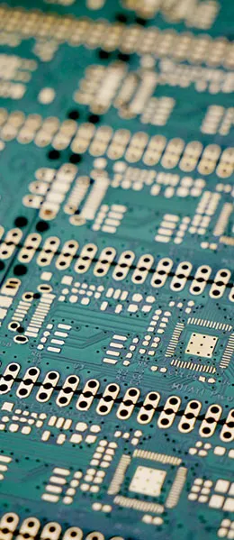
The field of printed circuit board (PCB) manufacturing has been constantly evolving to meet the demands of increasingly complex electronic devices. Plasma technology, as a high-energy, highly reactive medium, has been introduced into PCB manufacturing in recent years and has played a key role. This article will delve into the multifaceted roles of plasma in PCB manufacturing and provide you with detailed information about this technology.

Table of Contents
- What is plasma?
- The Role of Plasma in the PCB Manufacturing Process
- Bore Wall Pitting and Removal of Resin Deposits from Bore Walls
- Activation Treatment of Polytetrafluoroethylene (PTFE) Materials
- Carbide Removal
- Pre-treatment of PCB Inner Layers
- Removing the Electroplating Liner
- Frequently Asked Questions
- Conclusion
What is plasma?
Plasma is a high-energy, highly reactive state of matter, typically composed of ions and free electrons in a gas or other substance. It exhibits electrical and thermal conductivity, as well as extremely high chemical reactivity. This makes plasma highly promising for a wide range of applications across various fields, including PCB manufacturing.
Advanced: How is plasma generated, and what gases are used?
In industrial applications, plasma is not a “flame”; it isProcess gases are ionized using radio frequency or microwave energy inside the vacuum chamber.The resulting low-temperature plasma. Electrons, ions, and free radicals interact with the material surface, producing two types of effects:Physical Bombardment(breaking the molecular chains, roughening the surface) andChemical Reaction(Oxidation or reduction, resulting in volatile products).
- Oxygen (O₂): This is the most oxidizing solution; it is used to remove resin-based drilling debris, carbides, and organic residues, and is the most commonly used system.
- Argon (Ar): Inert; primarily relies on physical bombardment to clean and roughen surfaces; often used in combination with oxygen.
- Nitrogen / Hydrogen and Their Mixtures: Slightly reducing; used to prevent excessive oxidation or to treat oxygen-sensitive materials.
- Fluorinated gases such as carbon tetrafluoride (CF₄): Used for etching fluorinated materials or for special surface modification of PTFE-type materials.
The essence of selecting a gas system isStriking a Balance Between "Thorough Cleaning" and "Protecting the Substrate": A high oxygen concentration, high power, and long duration result in strong cleaning power, but they can also over-etch the resin on the pore walls, which in turn weakens the subsequent bonding strength.
| Gas Systems | Main Functions | Typical Applications | Points to Note |
|---|---|---|---|
| O₂ | Oxidative Degradation of Organic Compounds | Removing Contaminants and Carbides | Excessive use can cause excessive pitting. |
| Ar | Physical Blast Cleaning | Surface Roughening and Activation | When used alone, its cleaning power is weak. |
| O₂ + Ar | Synergy Between Chemistry and Physics | Most Common Combinations | Adjust the proportions based on the ingredients. |
| N₂ / H₂ | Reduction, Inhibition of Oxidation | Handling of Sensitive Materials | Explosion-proof management must be properly implemented. |
| CF₄ and other fluorinated gases | Fluorine Etching | Surface Modification of PTFE-Based Materials | Exhaust gases require special treatment |

The quality of holes that require cleaning is determined by the drilling process itself; for a related analysis, seeQuality Issues in the PCB Drilling Process。
The Role of Plasma in the PCB Manufacturing Process
Bore Wall Pitting and Removal of Resin Deposits from Bore Walls
In the PCB manufacturing process, it is typically necessary to etch the inner walls of the holes and remove resin contamination from them. This is done to ensure the quality of the hole walls and facilitate subsequent metallization plating. Traditional methods include treatment with concentrated sulfuric acid, chromic acid, and an alkaline potassium permanganate solution. However, for flexible printed circuit boards and rigid-flex printed circuit boards, these methods are of limited effectiveness.
Plasma treatment offers a better option for these special materials. It can achieve a favorable surface roughness on the pore walls, which facilitates metallization plating of the pores, while also providing “three-dimensional” etched bonding characteristics.
Activation Treatment of Polytetrafluoroethylene (PTFE) Materials
In PCB manufacturing, the surfaces of materials such as polytetrafluoroethylene (PTFE) require surface activation to enable electroless copper plating. Plasma treatment excels in this regard because it is a dry process that is easy to operate and delivers consistent, reliable results, making it suitable for mass production. In contrast, traditional chemical treatment methods require the synthesis of processing solutions and are associated with issues such as toxicity and a short shelf life.
Carbide Removal
As interconnect density increases, the demand for PCB manufacturing continues to grow, and laser technology has become a common method for creating blind vias. This process produces carbides. Plasma treatment technology has demonstrated superior performance in removing these carbides. Not only can it be used to clean various types of board materials, but it has also proven effective in removing contaminants from composite resin materials and micro-holes.
Pre-treatment of PCB Inner Layers
Surface pretreatment of the inner layers of flexible printed circuit boards and rigid-flex printed circuit boards is critical to successful manufacturing. Plasma treatment increases surface roughness and reactivity, improving the adhesion between the board’s inner layers and thereby enhancing the quality and reliability of the PCB.
Removing the Electroplating Liner
In some PCB manufacturing processes, the electroplating film may become trapped between the layers of the board. Plasma methods can also be used to address this issue by removing the trapped film, ensuring the highest quality of the finished PCB.
Advanced: What Does Each of the Five Application Scenarios Need to Control?
If we break down the five scenarios mentioned above, the control points for each scenario are actually different:
| Scene | What needs to be addressed? | Critical Control Points | Authentication Methods |
|---|---|---|---|
| Bore Wall Pitting and Drill Cuttings Removal | Remove resin residue caused by drilling heat to expose the inner copper layer | Pitting Depth, Hole Wall Roughness | Microscopic examination of sections, backlight inspection |
| PTFE Material Activation | Allowing Inert Surface Energy to Precipitate onto Electrolytic Copper | Surface Energy, Contact Angle | Electrolytic Copper Plating Coverage Integrity |
| Carbide Removal | Removing Carbon Residue from Blind Holes Drilled by Laser | Thorough decarbonization without damaging the medium | Slice and Adhesion Testing |
| FPC / Rigid-Flex Board Inner Layer Pretreatment | Improving Interlayer Bond Strength | Coarsening Uniformity, Processing Time | Peel Strength Test |
| Removing the Electroplating Liner | Remove any dry film residue trapped between the boards | Selectivity of the Site of Action | Visual Inspection and Sectioning |
There are three points that are most easily overlooked:
- The amount of etching should be moderate.: If the coating is too thin, the inner copper layer will not be sufficiently exposed, resulting in unreliable interlayer bonding; if it is too thick, the hole walls will be hollowed out, creating “wick-like” defects.
- Processing is subject to a time limit: The surface energy of the activated surface will decrease over time; therefore, after treatment, the material should proceed to the next process step as soon as possible and should not be exposed to the environment for an extended period.
- The clamping method affects uniformity: If the plates are stacked too closely together, with insufficient spacing, the plasma density in the central area will be insufficient, resulting in uneven processing of the entire batch.
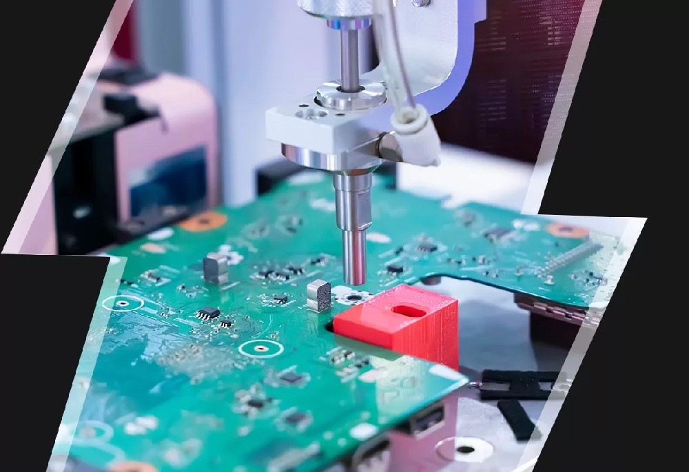

Advanced: A Direct Comparison with Wet Processes
| Comparison Items | Plasma (Dry Process) | Chemical Wet Process |
|---|---|---|
| Applicable Materials | Flexible plates, rigid-flex plates, PTFE, microporous materials with high aspect ratios | Primarily conventional rigid panels |
| Processing Uniformity | Okay, the inside and outside of the hole are the same. | Limited ability to replace the solution inside deep holes |
| Environmental Protection and Safety | No liquid waste, but vacuum and exhaust gas treatment are required. | Toxicity of Waste Liquids and Chemicals Requiring Treatment |
| Quality Consistency | Stable, with controllable parameters | Affected by the concentration of the solution and its shelf life |
| Batch Adaptation | Suitable for batch production; production capacity per batch is limited by the chamber size. | High production capacity |
| Cost Structure | High equipment costs | High costs for chemicals and waste liquid treatment |
From this, we can draw three very practical conclusions:
- High-Frequency and PTFE-Coated Plate-Priority Plasma: The wet method has limited effectiveness in activating PTFE, and the chemical solution system is also more complex;
- Plasma with a combination of flexible and rigid-flex plates: The wet process can cause the material to absorb moisture and swell, increasing the risk of delamination;
- It remains more cost-effective to continue using the wet process for standard rigid panels.: With lower costs and higher production capacity, there’s no need to force the adoption of the dry process.
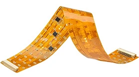
For information on processes related to flexible printed circuits, please refer toWhat Is an FPC (Flexible Printed Circuit)?与A Detailed Explanation of the Solder Mask Process for FPC Flexible Printed Circuit Boards。
Advanced: Five Steps to Pin the Process Window
The biggest risk with plasma treatment isn't that "it can't be done," but ratherInconsistencies between batches. To keep it under control, follow these five steps:
- Parameter Settings Window: The four parameters—power, gas ratio, chamber pressure, and processing time—must be determined together and included in the work instructions;
- First-Piece Verification: Use the slicing and weighing method (decontamination rate) to verify whether the treatment level meets the standards;
- Monitoring Uniformity: Place reference specimens at different locations within the chamber to compare the differences in the processing results;
- Time Limit: Specify the maximum allowable interval between the completion of a process and the start of the next process;
- Keep a record of the history: Record the parameters and test results for each batch to facilitate traceability in the event of a failure.

Advanced: When Is Plasma Treatment Necessary?
It is a valuable but not universally applicable process. It is worth explicitly specifying in the specifications only if it meets any of the following criteria:
- The materials are PTFE or high-frequency systems, the wet activation method is not very effective;
- The board is Flexible Slab or Rigid-Flex Slab, the wet method carries the risk of moisture absorption and swelling;
- 有 Laser Drilling of Blind Holes, the carbides at the bottom and on the walls of the hole must be removed;
- Small pore size and high diameter-to-wall-thickness ratio,It is difficult to thoroughly replace the solution;
- The product is used in high-reliability applications and requires greater stability.Interlayer Bond Strength。
If the process does not fall into any of the above categories, the wet process is generally more cost-effective. Incorporating plasma as a general-purpose step will only increase costs without providing any tangible benefits.
In applications involving high-density fiberboard, it is also commonly used withLaser DrillingRecommended procedure: First, drill the holes; then, use plasma to remove carbides and residual adhesive; finally, metallize the holes.
Frequently Asked Questions
Q: What are the advantages of plasma treatment compared to traditional methods?
Answer: Plasma treatment offers many advantages, including high efficiency, a dry process, consistent and reliable treatment quality, and suitability for mass production. It is particularly well-suited for treating special materials such as flexible printed circuit boards and rigid-flex printed circuit boards, where it delivers even better results.
Q: Is plasma treatment safe?
Answer: Plasma treatment is a relatively safe process. However, relevant safety guidelines must still be followed during operation, including the use of protective equipment and adherence to operating instructions.
Q: When is plasma treatment required in PCB manufacturing?
Answer: Plasma treatment is used in multiple stages of PCB manufacturing, including the etching of via walls, the activation of PTFE materials, the removal of carbides, the pretreatment of inner layers, and the removal of electroplating films. Specific requirements depend on the materials and processes used.
Q: Does plasma treatment alter the dimensions of the sheet metal?
Answer: Generally not. It is a surface treatment with a depth of action measured in micrometers or even submicrometers, so it does not cause any overall dimensional changes in the sheet material. This is also a major advantage over the wet method—which can cause moisture-induced swelling.
Q: How long can the treated boards be stored?
A: The activation effect diminishes over time; it is generally recommended toWithin a few hoursProceed to the next process step; the specific time limit is determined based on the materials and workshop conditions. If the time limit is exceeded, surface energy will decrease, affecting both the copper plating coverage and adhesion.
Q: Can plasma treatment replace chemical copper plating?
Answer: No. It addresses the question of whether the surface can be coated with copper, which is part of the pretreatment process; the actual formation of the conductive layer still relies on chemical copper plating and electroplating. These two processes are sequential steps, not substitutes for one another.
Q: What is an appropriate amount of etching?
Answer: In the industry, weighing or cross-sectional measurement is commonly used to determine this; the goal is toRemove the resin residue so that the inner copper ring is clearly visible, without hollowing out the hole walls.. Specific values are determined based on the material system and customer specifications; we recommend using the cross-section as a reference.
Q: Does plasma treatment make the pore walls too rough?
Answer: It does become rougher, and that is precisely how it improves adhesion. However, the roughness must be controlled—excessive roughness will cause discontinuities in the subsequent chemical copper plating, which in turn will create voids in the pore walls; therefore, both power and time must be adjusted together.
Q: Do all panel manufacturers have plasma equipment?
Answer: No. The equipment requires a significant investment, so typically only PCB manufacturers that produce high-frequency boards, flexible boards, and high-reliability products have this equipment. When selecting a manufacturer, you can ask them directly if they haveOur Plant's Equipmentas well as a track record of mass production for similar products.
Q: How much does plasma treatment increase costs?
Answer: The cost per batch is higher than that of the wet process, primarily due to equipment depreciation and capacity utilization. However, if this results inImproved bond strength between holes and walls; increased yield rate for high-frequency circuit boards in copper plating...the benefits gained from overall yield are often greater than the cost of the process itself.
Conclusion
Plasma technology plays a multifaceted role in PCB manufacturing, serving as a key process in applications ranging from via wall etching to surface activation and carbide removal. It offers an efficient, reliable, and mass-production-ready method, particularly well-suited for the processing of specialty materials. If you need more information about PCB manufacturing or plasma treatment, please feel free to contact me; I will be happy to provide you with support and consultation.
Further Reading:The Role of Ink in the FPC Manufacturing Process · 5 Key Requirements and Optimization Strategies for the HDI Manufacturing Process