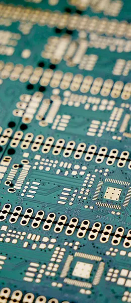
In PCB (printed circuit board) design, gold fingers are an important electrical interface found in many electronic devices. The proper handling and attention to detail regarding gold fingers determine the performance and reliability of the PCB. This article will take an in-depth look at the function of gold fingers, methods for handling them, and solutions to common problems.

Advanced: What's the Difference Between Hard Gold and Soft Gold?
The Golden Finger usesHard Gold (Hard Gold)... and are two distinct processes—they cannot be used interchangeably:
| Comparison Items | Hard Gold Plating | Electrolytic Nickel Immersion Gold (ENIG) |
|---|---|---|
| Process | Electroplating, containing gold-cobalt or nickel alloys | Chemical Vapor Deposition |
| Hardness and Wear Resistance | Tall, suitable for repeated insertion and removal | Low; not suitable for friction |
| Thickness | Thicker; can be customized based on the required number of insertion/removal cycles | Very thin, usually a few tenths of a micrometer |
| Cost | High (requires a large amount of gold) | 中 |
| Uses | Gold fingers, contact surfaces | Soldering surfaces, general pads |
- Hard gold relies on alloying elements to increase its hardness: Pure gold is very soft, but adding cobalt or nickel significantly improves its hardness and wear resistance;
- Thickness is determined based on the number of insertion and removal cycles.: The more times a component is plugged in and unplugged, the thicker the gold plating must be;
- Hard gold is not suitable for use as a welding surface.: Hard gold is less solderable than electroplated gold and is more expensive.
- Misconception 1: Using Soft Gold Instead of Hard Gold: The gold plating is too thin and cannot withstand the wear and tear caused by repeated insertion and removal;
- Misconception 2: The thicker the gold layer, the better: The thickness is determined by the number of insertion and removal cycles; making it too thick only increases costs;
- Misconception 3: Hard gold is also suitable for soldering: Hard gold has poor solderability; an alternative method should be selected for the pads.
A common misconception is to use the same surface treatment for gold fingers and pads.The demands of the two are exactly opposite.: Gold fingers need to be wear-resistant, and the pads need to be easy to solder. Therefore, the standard practice is to electroplate the gold finger areas with hard gold, while the remaining pads are either immersion-gilded or tin-plated.
See the "Golden Finger" Design GuideGuide to PCB Gold Finger Design and Manufacturing; see Surface PlatingA Detailed Explanation of the PCB Surface Plating Process。
The Role of the Golden Finger
Gold fingers are typically conductive contacts on a PCB used to connect to other electronic components, such as expansion cards or cables. They play a crucial role in PCB design. The following are their main functions:
1. Electrical Connections
Gold fingers enable electrical connections between PCBs and other electronic devices or components. These connections can be used for signal transmission, power supply, or other forms of data exchange.
2. Signal Transmission
In high-frequency applications, gold fingers are used to transmit precision signals. They require special processing to ensure signal accuracy and stability.
3. Electrostatic Discharge (ESD) Protection
Gold finger designs can also be used to prevent ESD damage to PCBs and related electronic devices. With proper treatment, gold fingers can serve as a protective barrier against ESD.
Advanced: Chamfer Parameters and Common Mistakes
The purpose of the chamfer is to allow the board to slide smoothly into the slot while preventing the connector from being scratched. Three parameters must be specified:
- Angle: The standard angle is 45°, though special requirements such as 30° may apply; the angle must match the slot specifications;
- In-Depth: The distance cut inward from the edge of the plate; cutting too deeply will damage the effective contact area;
- Direction: Specify whether the chamfer is on the front or back side; this is especially important for double-sided gold fingers.
| Error Type | Consequences | Prevention Methods |
|---|---|---|
| Angle not specified | Processing using the default settings may not match the slot. | The drawings clearly specify angles and tolerances. |
| Chamfer is too deep | Insufficient effective contact length; poor contact | Control the depth and allow for a margin in the contact area |
| Wrong Direction | Difficulty inserting or inability to insert | Use diagrams to indicate the chamfered surfaces |
| Missed Chamfer | The card cannot be inserted or has scratched the slot | Include chamfering as a mandatory inspection item in the process requirements |
Chamfering is one of those processes where you don’t realize you’ve made a mistake until it’s too late, because you can’t test-fit the board until it’s finished.Therefore, clearly indicate the chamfering requirements on the drawings and verify them through an actual test fit during the production of the first part....are the two key steps to avoiding large-scale rework.

For contour machining, seeMethods and Characteristics of Circuit Board Contour Machining; See the process edge specifications atStandards for Setting the Width of Process Margins on PCBs。
Details of the "Golden Finger"
In PCB design, attention to detail regarding gold fingers is crucial. Here are some important methods and considerations:
1. Hard Gold Plating
To increase the wear resistance of gold fingers, they are typically plated with hard gold. This ensures that the gold fingers will not wear out easily during prolonged use.
2. Chamfering
The edges of gold fingers typically require chamfering, usually at a 45° angle. This helps minimize functional loss caused by improper chamfering.
3. Solder Mask Cutouts
The area around the gold finger needs to be machined as a single piece.Solder MaskCut openings to ensure the reliability of the weld. No openings are required in the PIN section of the steel mesh.
4. Pad Spacing
Tin-plated and silver-plated pads must be at least 14 mils away from the tip of the gold finger. It is recommended that, during design, pads—including via pads—be placed at least 1 mm away from the gold finger.
5. Surface Treatment
The outer surface of the gold fingers should not be coated with copper to ensure the quality of the connection.
6. Copper Shaving Process
All layers within the gold finger must undergo copper removal; typically, the width of the copper removal is 3 mm. This helps reduce the impedance difference between the gold finger and the impedance lines, while also providing ESD protection.
7. Specify the correct chamfer specifications
Incorrect chamfering may result in the loss of some of the board's functions. Therefore, the chamfering specifications for gold fingers must be accurately specified, including the angle and depth.
Advanced: Four Distance Rules for the "Golden Finger" Area
The requirements mentioned in the original text—such as a 14-mil spacing, no copper plating, and copper removal—are essentially intended toPrevent other metals from affecting the contact and impedance of the gold fingers:
| Rules | Requirements | Purpose |
|---|---|---|
| Distance Between Pads and Gold Fingers | The minimum distance from the top of tin-plated or silver-plated pads is 14 mil; a distance of 1 mm or more is recommended. | Prevent solder contamination of the contact surfaces |
| No copper is applied to the surface layer | The surface layer of the "Golden Finger" area is not plated with copper. | Avoid interfering with insertion, removal, and contact |
| Inner-layer copper removal | Each inner layer is etched to remove copper, with a width typically greater than 3 mm | Reduce the impedance difference with the impedance line and improve ESD protection |
| Solder Mask Cutouts | Cut out the entire window; do not cut the steel mesh in the PIN section. | Ensure reliable contact and prevent solder mask residue |
- Pad spacing is a mandatory requirement.: If the distance is insufficient, solder may flow onto the gold fingers during the reflow process, causing a poor connection;
- Copper removal affects impedance.: The large area of copper beneath the "golden finger" will alter its characteristic impedance;
- The solder mask must be cut out in one continuous piece.: Opening windows in specific areas can leave behind solder mask residue.
These rules may seem trivial, but each one corresponds to a specific failure mode. In the design of the "golden fingers,"Enforce the rules as strict requirements, rather than treating them as mere guidelines....which can prevent the vast majority of contact-related issues.

See the Golden Rules of DesignThe Top 10 Golden Rules of PCB Design; For information on electrostatic protection, seeElectrostatic Protection Design for PCBs。
Advanced: ESD and Reliability Design for "Magic Fingers"
The gold fingers are one of the areas of the device most susceptible to electrostatic discharge—they are directly exposed and are most likely to become charged when people plug or unplug the device. The following design measures are typically taken:
- Extended Grounding Finger: Make the ground contact longer than the signal contact so that the ground connection is established first when plugging in and is disconnected last when unplugging;
- Set the release path: Place ESD protection components near the "golden finger" to divert the energy to ground;
- Inner-layer copper etching alignment: Improve the electric field distribution and reduce the risk of discharge damage;
- Enclosure Grounding Alignment: Allow static electricity to discharge through the chassis rather than through the circuitry on the board.
Of these, the first one is the most cost-effective and efficient approach.Those first few milliseconds when the finger makes contact with ground often determine whether static electricity will enter the signal circuit....This is a classic and effective technique in "Golden Finger" strategy.
- Confirm Slot Specifications: Contact definitions, length, and chamfer requirements;
- Defining Ground and Signal Sequence: Ground connection first;
- Placement of ESD Devices: Place it near the golden finger;
- First-piece insertion and discharge testing: Verified through actual testing.

Improvements in fingerprints are evidentMethods and Measures for Reducing Fingerprints on PCBs; For manufacturer quality information, seeWhich PCB manufacturer offers the best quality?。
Solutions to Common Problems
1. What should I do if there's a problem with the chamfer on the gold finger?
If there is a problem with the chamfer on the gold fingers, it may cause the board to malfunction. During the design process, ensure that the chamfer specifications are accurate and confirm them with the customer if necessary.
2. How can the soldering reliability of gold fingers be improved?
The soldering reliability of gold fingers can be improved through proper solder mask opening design and control of pad spacing.
3. How can you prevent wear and tear on the gold fingers?
Hard gold plating effectively prevents wear on gold fingers and extends their service life.
4. How can the impedance issue with the "golden finger" be resolved?
Copper milling can reduce the impedance difference between the gold fingers and the impedance lines, thereby improving the stability of signal transmission.
5. Does the design of the gold fingers affect ESD protection?
The design of the gold fingers can be used to enhance ESD protection and ensure that electronic devices are not damaged by ESD.
6. What is the typical thickness of a gold finger?
The thickness of the gold layer is determined based on the number of insertion/removal cycles and reliability requirements, ranging from several tens of microns to even greater values. The higher the number of insertion/removal cycles and the more severe the environmental conditions, the thicker the gold layer must be. Specific values should be clearly indicated on the drawings, and the manufacturer’s process capabilities should be confirmed, as thickness directly affects cost.
7. Can the "Golden Finger" be made double-sided?
Yes. Both sides of the double-sided gold fingers must be plated with hard gold and chamfered separately. Please note that the chamfering direction for both sides must be clearly marked, and requirements such as copper removal on the inner layer must apply to both sides. A double-sided design is more expensive and involves more complex process control.
8. Why can't traces be routed in the gold-finger area?
On the one hand, trace routing is affected by solder mask and hard gold plating; on the other hand, other metals beneath the gold fingers can alter their characteristic impedance and electric field distribution. Therefore, it is typically required that the outer layers remain copper-free and that the inner layers undergo copper reduction, leaving the gold finger area as a relatively “clean” region.
9. What should I do if the gold-plated connector is oxidized?
Gold itself does not oxidize easily; the problem is usually surface contamination or fingerprints. Minor contamination can be treated with a specialized cleaner; severe wear or contamination requires replacing the circuit board. Preventive measures include following standard operating procedures to avoid touching the surface with bare hands, ensuring proper packaging protection, and selecting an appropriate gold layer thickness during the design phase.
10. Can a gold-plated board be used directly as a gold finger?
No. The gold plating layer is very thin and not wear-resistant; after just a few insertions and removals, the underlying nickel layer will be exposed, leading to increased contact resistance and corrosion. Gold fingers must be made of electroplated hard gold; the manufacturing processes and thicknesses of the two are different, so they cannot be used interchangeably.
11. How do you control the impedance of a gold finger?
A "golden finger" is essentially a trace with a discontinuity in characteristic impedance; deviations must be minimized by reducing copper thickness, controlling finger width and spacing, and ensuring a properly designed reference plane. For high-speed interfaces, designs must typically comply with protocol specifications and undergo empirical verification during the prototype stage.
Conclusion
Gold fingers play a crucial role in PCB design, and proper attention to detail is essential. Methods such as hard gold plating, chamfering, solder mask openings, and controlling pad spacing can ensure the quality and performance of gold fingers. Attention to detail in the design process is key to ensuring optimal reliability and performance of the PCB.
Advanced: Testing and Acceptance of the "Golden Finger" Project
| Test Items | Methods | Common Nonconformities |
|---|---|---|
| Gold Layer Thickness | X-ray Thickness Measurement | Insufficient thickness |
| Coating Adhesion | Tape or Cross-Hatch Test | Peeling, flaking |
| Shapes and Chamfers | Projection or Microscopic Measurement | Angle Deviation, Depth Deviation |
| Appearance of the Contact Area | Visual Inspection or AOI | Scratches, Stains, and Residual Film |
| Position Dimensions | Coordinate Measurement | Finger Spacing Deviation |
| Test Installation | Test by inserting it into an actual slot | Difficulty inserting, poor contact |
- Test installation is the most effective way to verify acceptance.: Just because a drawing meets specifications doesn’t mean it’s usable; actually inserting it into the slot can immediately reveal issues with chamfers and dimensions;
- Random inspections of gold layer thickness are required: Insufficient thickness can lead to rapid wear during use and is considered a hidden defect;
- Packaging and protection must be included in the requirements.: Scratches and stains on gold fingers are common during shipping.

Related Recommendations:Guide to PCB Gold Finger Design and Manufacturing · Which PCB manufacturer offers the best quality?