

I. Unveiling the Mystery of Bonded Circuit Boards
In today’s electronics market, smartphone screens are getting larger while the devices themselves are becoming thinner, and smartwatches can integrate a variety of functions—such as heart rate monitoring and location tracking—yet remain compact and lightweight. Behind the realization of these “contradictions” lies a key technology: bonding technology—and bonded circuit boards are the core medium for this technology.
You might be wondering: What is a bonded PCB? How is it different from the traditional PCBs we’re familiar with? And why does it serve as an “unsung hero” in high-end electronic devices, quietly supporting their high-performance operation?
Whether you’re an electronics R&D engineer, a corporate procurement manager, or an enthusiast interested in electronics, this article will provide you with a clear understanding of the technical principles, key advantages, application scenarios, and selection criteria for bonded circuit boards—enabling you to make the most of them to meet your needs.
II. Basic Understanding: A Guide to Bonded Circuit Boards
(1) Analysis of Definitions
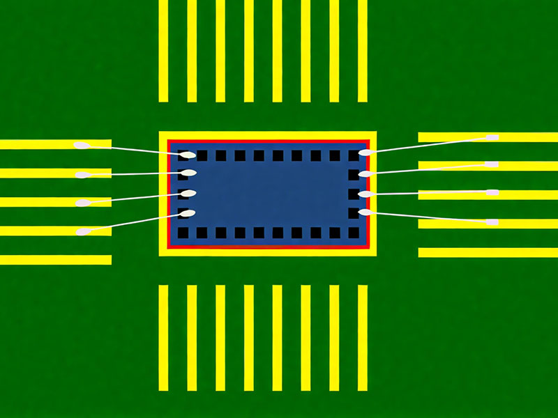
A bonded PCB is, simply put, a special type of printed circuit board in which the chip is directly bonded to the PCB substrate using a specific “bonding process.” Unlike traditional printed circuit boards, which rely on intermediate components such as connectors and leads to connect the chip to the substrate, bonded PCBs enable “zero-distance” contact between the chip and the substrate. Common bonding processes include COB (Chip On Board), COG (Chip On Glass), and TCP (Tape Carrier Package), This direct connection is the core feature that distinguishes bonded PCBs from other types of printed circuit boards.
(2) Core Components
The performance and stability of a bonded printed circuit board depend on the synergistic interaction of its key components, which primarily include the following four parts:
- Substrate: As the fundamental substrate of a printed circuit board (PCB), its material directly affects the PCB’s heat dissipation, insulation, and stability. Common substrate materials include FR-4 (epoxy-glass fiber substrate, suitable for general-purpose applications), ceramic (high thermal conductivity, suitable for applications with high heat dissipation requirements), and flexible materials (such as polyimide, which can be used in bendable devices).
- Chip: Depending on the bonding process, the type of chip and the mounting method also vary. For example, the COB process typically uses bare chips that are directly bonded to the substrate, while the COG process mostly uses driver chips that are bonded to a glass substrate.
- Bonding Adhesive: Its primary function is to protect the chip and its connection points by shielding them from external moisture and dust, while also cushioning the impact of vibrations on the chip. The material must possess good insulation properties, high-temperature resistance, and resistance to aging; common examples include epoxy-based bonding adhesives.
- Lead-in: In some bonding processes, such as COB, wires (typically gold or copper) are used to connect the chip to the substrate circuits; the diameter, material, and soldering quality of these wires directly affect the stability of signal transmission.
(3) Comparison with Traditional Printed Circuit Boards
To gain a clearer understanding of the characteristics of bonded circuit boards, we will compare them with traditional through-hole and surface-mount circuit boards based on four criteria: connection methods, size, performance, and cost:
|
Dimensions of Comparison
|
Bonded Circuit Board
|
Plug-in Circuit Boards
|
Surface-Mount Printed Circuit Board
|
|
Connection Methods
|
The chip is directly bonded to the substrate, eliminating the need for an intermediate connector.
|
The chip is connected by inserting its pins into the holes in the circuit board.
|
The chip is attached to the pads on the surface of the substrate using solder.
|
|
Volume
|
Compact size, reduces 30%-50%
|
Large size; pins and connectors take up a lot of space
|
Medium in size—smaller than a plug-in module, but larger than a bonded circuit board.
|
|
Performance
|
Short signal transmission path, low loss, and stable operation
|
The signal transmission path is long, making it susceptible to interference, and stability is generally average.
|
Signal transmission performance is better than that of plug-in types, but still not as good as that of bonded circuit boards.
|
|
Cost
|
Low long-term mass production costs (fewer parts and processes)
|
There are many parts, and the cost of manual assembly is high.
|
SMT equipment is expensive, and production costs are relatively high for small batches.
|
III. Core Technology: The “True Strength” of Bonded Circuit Boards”
(1) A Detailed Explanation of Mainstream Bonding Processes
Different bonding processes are suitable for different applications, and their principles and advantages vary depending on the specific context:
- COB (Chip On Board) Process: The core of this process involves directly bonding the bare chip to the substrate, then connecting the chip’s leads to the circuit traces on the substrate using gold or copper wires, and finally covering and protecting the assembly with bonding adhesive. Its greatest advantages lie in its compact size, which enables high integration, and its excellent heat dissipation performance, as the chip is in direct contact with the substrate, allowing heat to be rapidly conducted away. It is widely used in the LED lighting sector (such as LED chip arrays) and in power modules (such as compact switching power supplies).
- COG (Chip On Glass) Process: Primarily used in display devices, this technology involves directly bonding the display driver chip to a glass substrate, eliminating the need for traditional driver boards and connectors. This process simplifies the structure of the display module, reduces the number of signal transmission stages, thereby enhancing display quality and reducing screen thickness. Currently, most LCDs and touchscreens (such as those found in smartphones and tablets) utilize this process.
- TCP (Tape Carrier Package) Process: First, the chip is mounted on a flexible carrier tape (typically made of polyimide), which has pre-printed circuits, and then connected to the substrate via the pins on the carrier tape. The advantages of this process include high flexibility, which allows it to adapt to curved installation environments, as well as strong shock resistance. It is commonly used in applications such as laptop screens and image sensor connections in digital cameras.
(2) Key Technical Challenges and Solutions
The production process for bonded printed circuit boards involves several technical challenges. If not handled properly, these challenges can affect product quality. The following are common challenges and their corresponding solutions:
- Challenge 1: High bonding accuracy requirements (micrometer level); cold solder joints and misalignment are common
During the bonding process, the alignment accuracy between the chip and the substrate must be at the micrometer level. Any deviation can result in poor pin contact and cold solder joints; if the deviation is too great, it can even cause damage to the chip.
Solution: Use fully automated bonding equipment paired with a high-definition vision positioning system. The equipment uses a camera to capture the position data of the chip and substrate in real time, compares this data with preset parameters, and automatically calibrates the position, maintaining alignment accuracy within ±0.01 mm, thereby effectively preventing cold solder joints and misalignment issues.
- Challenge 2: Heat Dissipation After Bonding (Heat Concentration Due to Chip Density)
In highly integrated bonded circuit boards, multiple chips are densely packed together and generate a significant amount of heat during operation. If this heat cannot be dissipated quickly enough, it can cause the chips to overheat, affecting performance or even causing damage.
Solution: Optimize the thermal design in several ways. First, select a substrate material with high thermal conductivity, such as a ceramic substrate, which has a thermal conductivity more than 10 times that of an FR-4 substrate. Second, design ventilation holes in the substrate or apply a thermal-dissipating coating to enhance heat dissipation; Finally, optimize the circuit layout to avoid clustering high-power-consumption chips, thereby reducing heat buildup.
IV. Advantages and Applications: Why Are Bonded Circuit Boards So “Popular”?”
(1) Identifying Core Strengths
The widespread use of bonded circuit boards in numerous electronic devices is primarily due to their four core advantages:
- Space Advantages: By directly bonding the chip to the substrate, the installation space required for components such as connectors and leads is eliminated, significantly reducing the size of the circuit board. Compared to traditional circuit boards, bonded circuit boards can be up to 30%–50% smaller, which is crucial for electronic devices that prioritize miniaturization, such as smartwatches and Bluetooth earbuds.
- Performance Advantages: Direct bonding of the chip to the substrate shortens the signal transmission path, reduces signal loss and interference during transmission, and thereby improves the device’s operating speed and stability. For example, in smartphone camera modules, the use of bonded circuit boards enables rapid transmission of image signals, reduces latency, and enhances photo quality.
- Cost Advantage: On the one hand, it reduces the use of components such as connectors and leads, thereby lowering material costs; on the other hand, it simplifies the production process, reduces manual assembly steps, and improves production efficiency. In long-term mass production, the cost of bonded circuit boards can be 15%-20% lower than that of traditional circuit boards.
- Reliability Advantages: Bonding adhesive tightly encapsulates the chip and connection points, shielding them from external moisture, dust, and corrosive gases, while also cushioning the impact of vibrations on the chip. In harsh environments, such as industrial workshops and vehicle interiors, bonded circuit boards have a longer service life and higher reliability than traditional circuit boards.
(2) Typical Application Scenarios
Thanks to these advantages, bonded circuit boards are now widely used in a variety of fields, including consumer electronics, industrial control, automotive electronics, and medical electronics:
- Consumer Electronics Sector: In smartphones, camera modules and RF modules use bonded circuit boards to achieve miniaturization and high performance; the processors in smartwatches are bonded using the COB process to ensure proper operation in confined spaces; and the display driver boards in tablets rely on the COG process to enable thin-screen designs.
- Industrial Control Sector: Industrial sensors require high-precision detection modules; the high stability of bonded circuit boards ensures the accuracy of detection data; the core chip of the PLC controller is integrated using bonding technology, which improves the controller’s response speed; the mainboards of automated equipment use bonded circuit boards, enabling them to withstand the vibrations and high temperatures typical of industrial workshops.
- Automotive Electronics Sector: The driver board for the in-vehicle display uses COG technology to reduce screen thickness and enhance display quality; automotive-grade sensors require high-temperature-resistant circuit boards. Bonded circuit boards, which utilize special substrate materials and bonding adhesives, can operate reliably within a temperature range of –40°C to 125°C.
- The field of medical electronics: The micro-detection module in blood glucose meters relies on bonded circuit boards to achieve a compact design, making them easy to carry; the signal processing board in electrocardiogram machines uses bonding technology to reduce signal interference and ensure the accuracy of test data; the core chip in portable ultrasound devices is integrated using bonding, which reduces the device’s size and makes it easier for medical staff to use on the go.
V. Selection and Procurement: Avoiding the “Pitfalls” of Bonded Circuit Boards”
(1) Key Selection Criteria
When selecting a bonded PCB, you should consider your specific application requirements and focus on the following key metrics:
- Substrate Material: Select the appropriate substrate based on the application environment. For general-purpose consumer electronics, FR-4 substrates offer the best value; for devices with high power consumption and significant heat dissipation requirements—such as power supply modules—ceramic substrates should be chosen; and for devices that require bending—such as the flex cables in foldable smartphones—flexible substrates should be used.
- Bonding Process: Select the process based on the product’s functionality. To achieve high integration and a compact size, the COB process is the preferred choice; for display-related products, such as screens and touchscreens, the COG process is the best option; and for applications requiring flexible connections, such as bendable device components, the TCP process is more suitable.
- Accuracy Class: The precision grade must be determined based on the chip size. When the chip size is less than 1 mm, a bonding PCB with a precision of ±0.01 mm must be selected to ensure connection stability; when the chip size is between 1 and 5 mm, a product with a precision of ±0.05 mm will meet the requirements.
- Environmental Adaptability: Consider the equipment’s operating temperature, humidity, and vibration resistance requirements. For automotive-grade equipment, select bonded circuit boards capable of withstanding a temperature range of –40°C to 125°C; Industrial equipment typically requires operation within a temperature range of –20°C to 85°C; regarding humidity, it generally must be capable of withstanding an environment of 90% relative humidity (RH) without condensation; the vibration resistance rating must be determined based on the equipment’s installation environment—for example, printed circuit boards installed inside vehicles have higher vibration resistance requirements than those used in indoor equipment.
(2) A Guide to Avoiding Pitfalls in Procurement
When purchasing bond-mounted circuit boards, if you focus solely on price or overlook the details, it’s easy to run into problems. Here are three common “pitfalls” and corresponding tips for avoiding them:
- Pitfall 1: Focusing Only on Price and Ignoring Process Stability
To reduce costs, some procurement personnel opt for low-priced products; however, such products may fail to meet manufacturing standards or have inconsistent quality, which can lead to issues such as cold solder joints or damage during subsequent use, thereby actually increasing repair costs.
Recommendation: When purchasing, do not focus solely on price; request that suppliers provide samples for testing, such as high- and low-temperature cycling tests (to simulate stability under different temperature conditions) and vibration tests (to assess vibration resistance); At the same time, review the supplier’s process certifications, such as ISO 9001 Quality Management System certification and IATF 16949 automotive-grade certification, to ensure that their production processes are standardized and consistent.
- Pitfall 2: Lack of Clear After-Sales Service Makes It Difficult to Resolve Issues
Some procurement contracts do not clearly specify after-sales service terms. When quality issues arise with the products, suppliers may shirk responsibility, resulting in delays in resolving the problems and affecting production schedules.
Recommendation: When signing a purchase contract, clearly specify the warranty period (generally at least one year), the return and exchange policy (e.g., the number of days the supplier has to process returns or exchanges in the event of quality issues), and the technical support response time (e.g., the supplier must provide technical support within 24 hours in the event of equipment failure) to protect your rights and interests.
- Pitfall 3: Ignoring the supplier’s production capacity, which affects delivery times
If a supplier lacks sufficient production capacity, it may be unable to deliver on time, which could delay the company’s production schedule and result in financial losses.
Recommendation: Before making a purchase, conduct an on-site inspection of the supplier’s production facility to assess the number of machines (at least five fully automatic bonding machines are required to meet mass production needs) and the average daily production capacity (which must be ≥5,000 wafers per day to ensure timely delivery). Select a supplier with stable production capacity.
VI. Industry Trends: The “Future Direction” of Bonded Circuit Boards”
(1) Trends in Technological Upgrades
With the continuous advancement of electronic technology, bonding circuit board technology is also undergoing constant upgrades, and three major trends are expected to emerge in the future:
- A More Precise Bonding Process: As chip sizes continue to shrink (with 3nm and 2nm chips gradually becoming more widespread), the requirements for bonding accuracy will also become more stringent. In the future, bonding processes will achieve breakthroughs in nanometer-level precision. At the same time, the vision-based positioning systems and calibration technologies of fully automated bonding equipment will continue to be optimized to ensure higher bonding accuracy.
- Multifunctional Integration: Traditional bonded circuit boards primarily connect single chips; in the future, the industry will evolve toward “system-in-package” (SiP) technology, which integrates various functional chips—such as sensors, processors, and memory—onto a single substrate using bonding technology to form a complete functional module, thereby further enhancing the integration and performance of devices.
- Environmentally Friendly Processes: Against the backdrop of increasingly stringent environmental policies, the production of bonded circuit boards will place greater emphasis on environmental sustainability. On the one hand, lead-free bonding solders will be developed to replace traditional leaded solders, thereby reducing heavy metal pollution; on the other hand, biodegradable bonding adhesives will be developed to minimize environmental impact and ensure that products comply with environmental standards such as RoHS and REACH.
(2) Market Trends
In terms of market demand, the demand for bonded circuit boards is expected to continue growing across multiple sectors:
- Consumer Electronics Sector: With the growing popularity of foldable smartphones and wearable devices (such as smart bracelets and smart glasses), demand for flexible bonded circuit boards is expected to increase significantly, with an annual growth rate projected to reach 25%. At the same time, the trend toward higher performance in consumer electronics will also drive the adoption of highly integrated bonded circuit boards.
- Automotive Electronics Sector: The electrification rate of new energy vehicles continues to rise, increasing from 30% in traditional vehicles to 60%. Demand for bonded circuit boards for components such as in-vehicle displays, automotive-grade sensors, and autonomous driving modules will also continue to grow, and the market size for automotive-grade bonded circuit boards is expected to expand rapidly.
- The field of medical electronics: As people place greater emphasis on health management, demand for portable medical devices (such as portable blood pressure monitors and fetal heart rate monitors) continues to grow. These devices place high demands on printed circuit boards in terms of miniaturization and high precision, making miniaturized bonded printed circuit boards a core component with enormous market potential.
VII. Frequently Asked Questions (FAQ)
1. What should you do if there are cold solder joints on a bonded circuit board?
When solder joints on a bonded circuit board are defective, the first step is to identify the cause. There are three common causes: First, insufficient bonding temperature, which prevents the solder from melting completely; second, insufficient bonding pressure, resulting in poor contact between the chip and the substrate; and third, oxidation of the pads, which impairs solder adhesion.
Depending on the cause, appropriate solutions can be implemented: If the temperature is too low, increase the bonding temperature by 5–10°C based on the solder’s melting point (be careful not to set the temperature too high to avoid damaging the chip); If the pressure is insufficient, increase the bonding pressure appropriately, maintaining it between 0.1 and 0.3 MPa; if the pads are oxidized, wipe them with alcohol to remove the oxide layer before rebonding.
2. Can bonded circuit boards be repaired?
The difficulty of repairing bonded circuit boards depends on the bonding process and the size of the chip:
For small-scale chip bonding (such as bare chips in the COB process), because the chips are small and covered with bonding adhesive, it is difficult to precisely remove and rebond them during repairs. Since repairs are challenging, it is generally recommended to replace the entire circuit board to ensure the stability of the equipment.
For large chips or modular bonding (such as chips in the TCP process), since the chips are large and the bonding method is relatively simple, it is possible to remove the old chip using specialized bonding equipment, clean the substrate, and rebond a new chip. However, the repair cost is high—approximately 60% of the cost of a new circuit board—so the decision to repair should be weighed against the product’s value.
3. What is the service life of a bonded circuit board?
The service life of bonded circuit boards is significantly affected by the operating environment:
Under normal operating conditions (room temperature, dry environment, no severe vibration)—such as for consumer electronics used indoors—the service life is generally 3–5 years; in industrial and automotive environments, however, due to the longer service life of the equipment and the more durable materials and manufacturing processes used in bonded circuit boards, the service life can reach 8–10 years.
When used in harsh environments (high temperature, high humidity, frequent vibration)—such as near high-temperature equipment in industrial workshops or components near automotive engines, the service life of bonded circuit boards may be shortened—potentially to as little as 2–3 years. In such cases, regular inspections (recommended every 6 months) are necessary to promptly replace aging circuit boards and prevent equipment failures.
