

The quality and reliability of a PCB determine the quality and reliability of the entire device. However, due to cost and technical constraints, PCB manufacturers may encounter PCB failures during production and use.
To address this type of failure, we need to employ some common failure analysis techniques to ensure a certain level of quality and reliability during PCB manufacturing. This article summarizes the top ten failure analysis techniques for reference.
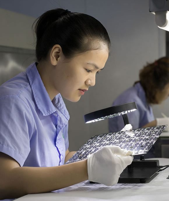
1. Visual Inspection
A visual inspection involves examining the appearance of a PCB by eye or using simple instruments to identify areas of failure and related physical evidence. Its primary purpose is to locate the failure and make a preliminary determination of the PCB’s failure mode.
2. X-ray fluoroscopy
For certain areas that cannot be detected through visual inspection, as well as the interiors of PCB through-holes and other internal defects, an X-ray inspection system must be used. An X-ray inspection system generates images based on the principle that different materials absorb or transmit X-rays at different rates depending on their thickness or density.
3. Section Analysis
Cross-section analysis is the process of obtaining the cross-sectional structure of a PCB through a series of methods and steps, including sampling, embedding, sectioning, polishing, etching, and observation. Cross-section analysis provides a wealth of information on the microstructure that reflects the quality of the PCB (such as through-holes and plating), offering a solid basis for subsequent quality improvements.
4. Scanning Acoustic Microscope
Currently, the primary instruments used for electronic packaging or assembly analysis are C-mode ultrasonic scanning acoustic microscopes. These instruments generate images by detecting changes in amplitude, phase, and polarization caused by the reflection of high-frequency ultrasonic waves at material discontinuities; they scan information in the X-Y plane along the Z-axis.
5. Microscopic Infrared Analysis
Microscopic infrared analysis is an analytical method that combines infrared spectroscopy with microscopy. It utilizes the principle that different materials (primarily organic compounds) absorb infrared spectra differently to analyze the chemical composition of materials. By combining this with a microscope, visible light and infrared light can share the same optical path, allowing for the detection of trace amounts of organic pollutants within the visible field of view.
6. Scanning Electron Microscopy Analysis
The scanning electron microscope (SEM) is one of the most useful large-scale electron microscopy imaging systems for failure analysis. In the analysis of PCB or solder joint failures, the SEM is primarily used to analyze failure mechanisms, specifically, it is used to observe the surface topography of pads, examine the metallographic structure of solder joints, measure intermetallic compounds, analyze solderability plating, and perform tin whisker analysis and measurements.
7. X-ray Spectroscopy
The scanning electron microscopes mentioned above are generally equipped with X-ray spectrometers. When a high-energy electron beam strikes the sample surface, inner-shell electrons in the atoms of the surface material are knocked out, and as outer-shell electrons transition to lower energy levels, they emit characteristic X-rays. Since the energy level differences vary among different elements, the characteristic X-rays emitted also differ; therefore, the characteristic X-rays emitted by the sample can be used for chemical composition analysis. Additionally, depending on whether the detected X-ray signals are based on characteristic wavelength or characteristic energy, the corresponding instruments are referred to as wavelength-dispersive spectrometers (WDS) and energy-dispersive spectrometers (EDS), respectively. WDS instruments offer higher resolution than EDS instruments, while EDS instruments provide faster analysis speeds than WDS instruments. Because EDS systems are fast and cost-effective, most scanning electron microscopes (SEMs) are equipped with EDS systems.
8. X-ray Photoelectron Spectroscopy (XPS) Analysis
When a sample is exposed to X-rays, inner-shell electrons of surface atoms are released from the atomic nucleus and escape from the solid surface to form photoelectrons. By measuring their kinetic energy (Ex), the binding energy (Eb) of the atom’s inner-shell electrons can be determined; Eb varies depending on the element and the electron shell. It serves as a “fingerprint” parameter for the atom, and the resulting spectral lines constitute the photoelectron spectroscopy (XPS) spectrum. In PCB analysis, XPS is primarily used to assess the quality of pad plating, identify contaminants, and determine the degree of oxidation, in order to pinpoint the underlying causes of poor solderability.
9. Thermal Analysis: Differential Scanning Calorimetry (DSC)
The DSC is equipped with two sets of compensation heating wires located beneath the sample and reference containers. When a temperature difference ΔT arises between the sample and the reference material due to thermal effects during the heating process, the current flowing through the compensation heating wires is modulated via a differential thermal amplification circuit and a differential thermal compensation amplifier. This balances the heat on both sides, eliminating the temperature difference ΔT, and records how the difference in thermal power between the two compensation heating wires beneath the sample and the reference material varies with temperature (or time). Based on this relationship, the physicochemical and thermodynamic properties of the material can be studied and analyzed. DSC has a wide range of applications; however, in the analysis of PCBs, it is primarily used to measure the degree of curing and the glass transition temperature of the various polymeric materials used in PCBs. These two parameters determine the reliability of the PCB in subsequent manufacturing processes.
10. Thermomechanical Analyzer (TMA)
Thermal Mechanical Analysis (TMA) is used to measure the deformation properties of solids, liquids, and gels under thermal or mechanical stress at program-controlled temperatures. Common loading methods include compression, penetration, tension, and bending. TMA has a wide range of applications. In PCB analysis, it is primarily used to determine the two most critical parameters: the coefficient of linear expansion and the glass transition temperature. PCBs made from substrates with excessively high coefficients of linear expansion often experience metallized via fractures and failures after soldering and assembly.
Due to the trend toward high-density PCBs and environmental requirements for lead-free and halogen-free manufacturing, an increasing number of PCBs are experiencing various failure issues, such as poor wetting, board delamination, delamination, and CAF. This article introduces the application of these analytical techniques in real-world cases at PCB manufacturers. Understanding the mechanisms and causes of PCB failures will facilitate future quality control efforts and help prevent similar issues from recurring.
Frequently Asked Questions
1. How long does it take to complete a PCB failure analysis?
The time required for PCB failure analysis depends on the complexity of the issue and the analytical techniques used. Generally speaking, simple issues may take only a few hours, while complex issues may take several days or even longer.
2. How do you choose the right failure analysis technique?
The selection of an appropriate failure analysis technique depends on the specific circumstances. First, the problem must be preliminarily identified, and then the appropriate technique must be selected based on the nature of the problem. Sometimes, a combination of techniques is necessary to thoroughly analyze the problem.
3. Can failure analysis completely resolve PCB issues?
Failure analysis can help identify and understand the root causes of problems, but the process of resolving them may require further engineering improvements and optimization. Failure analysis is the first step in problem-solving.
4. Is PCB failure analysis applicable to all types of electronic devices?
PCB failure analysis technology is applicable to various types of electronic devices, including consumer electronics, industrial equipment, and communications equipment. Regardless of the device’s size, failure analysis can help improve reliability and performance.
5. Can failure analysis be used for preventive maintenance?
Yes, failure analysis can be used for preventive maintenance. By conducting regular failure analysis on PCBs, potential problems can be identified early, and measures can be taken to prevent equipment damage and downtime.
