

The process of manufacturing printed circuit boards (PCBs) includes a critical testing phase. Every circuit board must be tested before leaving the facility to ensure that the manufacturer can detect any electrical or circuit issues. When a PCB passes this test, it further ensures its reliability. The most common testing methods include in-circuit testing (ICT) and flying probe testing (FPT).
Flying-probe testing is a high-precision and advantageous method for testing printed circuit boards using probes during the manufacturing process. As the number of small electronic devices continues to grow, it is becoming increasingly popular. Learn more about flying-probe testing and its benefits.
What is flying probe testing?
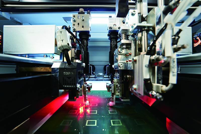
Fly-probe testing refers to the process of testing printed circuit boards during manufacturing using probes that “fly” toward the test points.
A flying-probe tester uses one or more test probes. These probes can make contact with test points on the circuit board from both the top and bottom. They then move from one location to another on the circuit board to test multiple wires or components.
They operate according to a program that outlines the specific circuit board being tested. These machines use high-precision probes to ensure the PCB functions properly. These systems do not require any test fixtures or custom tools. The probes have virtually no limitations in accessing the circuit board and can test boards with countless conductors. This makes flying probe testing a cost-effective option for circuit boards in the early stages of development. FPT is also well-suited for low- to medium-volume production.
Many people consider flying-probe testing to be the most proven method for testing printed circuit boards. It can perform the following non-destructive tests:
Capacitors, diodes, inductors, open circuits, resistors, short circuits—this testing method has been in use for more than 20 years, longer than other methods such as PCB testing.
What is test fixture testing?
A test fixture is a system that uses individual probes to make contact with each test point on a printed circuit board. These fixtures check for any assembly defects and verify proper functionality.
ICT is better suited for high-volume production because each PCB assembly requires custom test fixtures. Due to the complexity of printed circuit board assembly, these fixtures are typically very expensive.
Both circuit board testing and flying probe testing are effective methods for testing PCB performance.
How Flying-Probe Testing Works
The flying-needle test process is relatively simple and can be divided into the following three steps:
Step 1: Before you begin, you must create a test program for flying-probe testing. Test programs are typically developed using test program generation software on an offline PC. These programs generally require the following components:
Gerber files, Bill of Materials (BOM), Electronic Computer-Aided Design (ECAD) files. The BOM should be in Excel format, while the ECAD files must be CAD files.
Step 2: After creating the test program, it can be loaded onto the conveyor belt inside the test equipment. The circuit boards move along the conveyor belt to the test area, where probe operations are performed. There may be a single circuit board or multiple ones; the test will be controlled by the program.
Step 3: The probes can “fly” across the circuit board according to the test program. They use test signals to perform electrical and functional tests at various points on the circuit board. The measurement results are then processed to determine whether specific circuit sections meet expectations.
If the circuit board does not produce the expected results or deviates from the set program, the probe will send a signal indicating that the unit is defective and has therefore failed the test.
9 Advantages of Flying Probe Testing
Fly-probe testing offers many advantages. The following are some of the most important benefits of incorporating fly-probe testing into the printed circuit board assembly process:
Cost-Effectiveness
Compared to alternative methods such as printed circuit board testing, flying probe testing is a more cost-effective approach, especially when testing small-volume products.
Low upfront costs
Compared to PCB testing, flying probe testing has lower upfront costs because it does not involve expenses related to test fixtures.
Suitable for small- to medium-scale production
Due to their low development costs and short development time, flying-probe testing is ideal for low-volume production. Although they are not suitable for mass production, they can still be used for samples and prototypes.
Greater flexibility
The automation of flying-probe testing allows for greater flexibility in making test changes. Although there are some limitations with more complex tests, this approach is still beneficial.
Accuracy and Precision
Test probes can be precisely positioned, offering high accuracy and reliability. Flying probes are extremely precise and help prevent defects in finished products.
Short development time
The runtime of a flying-probe test varies depending on the size of the board. In most cases, the test takes approximately five to fifteen minutes per board.
High-Tech Features
Flying-probe testing now includes high-tech features such as the phase difference measurement (PDM) unit and micro-short-circuit detection.
Fewer customization tools
Fly-probe testing does not require custom tools like those used in PCB testing, which reduces upfront costs and time to market.
Best Examination
Because of its extremely high accuracy, you can combine flying-probe testing with automated optical inspection (AOI) to verify the correct layout and placement of each component on the printed circuit board.
Other Considerations for FPT
When using flying probe testing, there are several factors to consider in order to improve its accuracy and reduce the risk of damage to the PCB, including the following:
Cleanliness
Keeping the test area clean is essential for reducing test time and improving the reliability of the results.
Dimensions
Keeping access points close together can reduce test time, especially for large circuit boards.
Probe Contact Point
Easily accessible probe contacts can reduce costs and shorten test time.
