

What is electrochemical nickel-palladium-gold (ENEPIG)?
In the field of high-end electronics manufacturing, the surface treatment process for PCBs (printed circuit boards) directly determines the reliability and service life of the product. Chemical nickel-palladium-gold (ENEPIG, Electroless Nickel, Electroless Palladium, Immersion Gold)—a non-selective surface treatment technology—has become the preferred solution for numerous high-end applications thanks to its unique multi-layer plating structure.
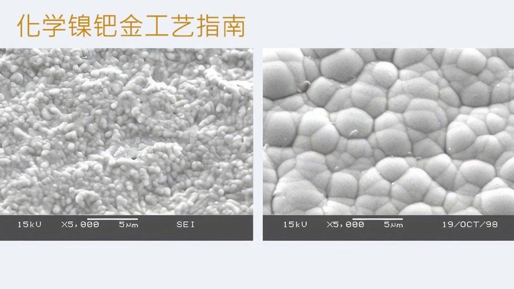
Its core principle involves using chemical deposition to sequentially form a three-layer protective coating—“nickel layer–palladium layer–gold layer”—on the bare copper surface of a PCB: The bottom nickel layer (typically 2–5 μm thick) provides a physical barrier for the copper surface, preventing the diffusion of copper atoms; the intermediate palladium layer (0.1–0.5 μm thick) serves as a critical “transition layer,” preventing oxidation of the nickel layer while enhancing the bond strength between the gold and nickel layers; The top gold layer (0.05–0.15 μm thick) imparts excellent solderability and electrical conductivity to the surface while providing protection against external corrosion. The synergistic effect of this multilayer structure enables the PCB to maintain stable performance even in complex environments.
A Comprehensive Analysis of the Electrolytic Nickel-Palladium-Gold (ENEPIG) Process
The process steps for chemical nickel-palladium-gold plating are closely interlinked, and the control of parameters at each step directly affects the quality of the plating. The standard process primarily consists of three major stages: pretreatment, core deposition, and post-treatment. The specific steps are as follows:
Pre-treatment: Laying a “Clean Foundation” for the Coating”
The primary goal of pretreatment is to remove impurities and the oxide layer from the copper surface of the PCB to ensure uniform adhesion of subsequent plating layers. The first step is the degreasing process: the PCB is immersed in an alkaline degreasing agent (pH 10–12, temperature 40–50°C) for 3–5 minutes. This chemical reaction dissolves organic impurities such as grease and fingerprints from the copper surface. The PCB is then rinsed three times with pure water to remove any residual degreaser.
Next comes the micro-etching process: A micro-etching solution containing sodium persulfate or a sulfuric acid–hydrogen peroxide system is used to lightly etch the copper surface at room temperature (etching depth: 0.5–1 μm). The purpose is to remove the natural oxide layer from the copper surface while creating a rough microstructure — — This roughened structure increases the contact area between the plating layer and the copper surface, thereby enhancing adhesion. After micro-etching, the surface must also be rinsed 2–3 times with pure water to ensure it is clean.
Finally, the pre-activation process: The PCB is immersed in dilute hydrochloric acid or a specialized activator (at a temperature of 25–30°C for 1–2 minutes) to activate the chemical reactivity of the copper surface, thereby creating favorable reaction conditions for subsequent nickel plating and preventing poor adhesion of the plating layer due to insufficient surface reactivity of the copper.
Core Deposition: A three-layer structure consisting of “nickel – palladium – gold” is formed sequentially
The electroless nickel plating process is the first critical plating layer: The pretreated PCB is immersed in an electroless nickel bath (mainly composed of nickel sulfate and sodium hypophosphite, with a pH of 4.5–5.5, temperature 80–90°C). Through a chemical reaction, nickel ions are reduced and deposited onto the copper surface, forming a uniform nickel layer. The deposition time is typically 5–10 minutes, and both temperature and time must be strictly controlled—too low a temperature will result in slow deposition and uneven thickness of the nickel layer, while too high a temperature may cause the nickel solution to decompose, producing impurities that affect the quality of the plating.
This is followed by the palladium plating process: the PCB, after nickel plating, is transferred to a palladium plating bath (mainly composed of palladium chloride and amine complexing agents, with a pH of 8–9 and a temperature of 40–50°C). The palladium ions in the solution undergo a displacement reaction on the surface of the nickel layer, forming a dense palladium layer. The key to this step is controlling the thickness of the palladium layer: if it is too thin, it cannot effectively prevent oxidation of the nickel layer; if it is too thick, it increases costs. The deposition time is typically 2–4 minutes to ensure the palladium layer thickness remains between 0.1 and 0.5 μm.
Finally, the gold plating process: A displacement gold solution (whose main components are potassium gold cyanide or gold thiourea salt, with a pH of 5–6, temperature 30–40°C) to induce a displacement reaction between the gold ions and the palladium layer, forming a thin, uniform gold layer on the surface of the palladium layer. The thickness of the gold layer is typically controlled between 0.05 and 0.15 μm—it does not need to be too thick, as the palladium layer already provides sufficient protection. A thin gold layer ensures weldability while significantly reducing costs, and the deposition process can be completed in 1–3 minutes.
Post-Treatment: Ensuring a Stable and Reliable Coating
After the core deposition is complete, post-treatment is required to further enhance the stability of the plating layer. The first step is the rinsing process: Rinse 3–4 times with pure water to thoroughly remove any residual chemicals from the PCB surface (especially cyanide residues left after electroless gold plating, which must be thoroughly rinsed away). Each rinse should last 1–2 minutes, and the water temperature should be maintained at room temperature to prevent discoloration of the plating caused by high temperatures.
Next is the drying process: Place the washed PCBs in a hot-air drying oven (temperature 60–80°C, airflow speed 2–3) and dry them for 5–8 minutes to ensure no moisture remains on the PCB surface — — If moisture remains, it may cause bubbles or oxidation spots in the plating, affecting both appearance and performance. After drying, the PCBs must be cooled to room temperature before undergoing visual inspection and subsequent processing.
The Four Key Performance Advantages of Electrolytic Nickel-Palladium-Gold (ENEPIG)
Exceptional Corrosion Resistance and Reliability: Withstanding Challenging Environments
In applications such as automotive electronics and industrial control, PCBs are often exposed to harsh conditions such as high temperatures, high humidity, and vibration; the multi-layer structure of chemical nickel-palladium-gold plating provides exceptional protection. The presence of the intermediate palladium layer is key—it effectively prevents the nickel layer from coming into contact with air and water vapor, thereby preventing oxidation of the nickel layer and the formation of “nickel rust.” At the same time, the gold layer itself possesses excellent chemical inertness, enabling it to withstand corrosion from acids and alkalis.
Taking automotive engine control units (ECUs) as an example, PCBs treated with a chemical nickel-palladium-gold plating process maintain stable conductivity even after 1,000 cycles in temperature cycling tests ranging from –40°C to 125°C; In salt spray testing (5% NaCl solution at 35°C), no significant signs of corrosion were observed within 72 hours, far outperforming traditional processes such as tin plating and OSP. This is the key reason why it has become the preferred surface treatment process for automotive electronics.
Excellent weldability and compatibility: Suitable for a wide range of welding needs
In high-end electronics manufacturing, solderability directly affects soldering yield, and the top-layer gold coating of chemical nickel-palladium-gold provides excellent wettability for the solder — — During the reflow soldering process, the gold layer rapidly fuses with the solder to form a strong solder joint, without exhibiting “gold brittleness” (because the gold layer is thin, the palladium layer suppresses excessive reactions between gold and tin).
At the same time, it is fully compatible with environmentally friendly soldering requirements: Whether using lead-free solder (melting point 217°C) or traditional leaded solder (melting point 183°C), the chemical nickel-palladium-gold plating maintains stable performance and does not peel off or degrade due to fluctuations in soldering temperatures. Furthermore, it supports the “gold wire bonding” process; in semiconductor chip packaging, the gold layer forms a reliable bond with the gold wire, meeting the signal transmission requirements between the chip and the PCB.
Reasonable Cost Control: Balancing Performance and Value for Money
Compared to the “electroless gold” (ENIG) process, chemical nickel-palladium-gold offers a cost advantage. The ENIG process relies on a relatively thick gold layer (typically 0.1–0.2 μm) to ensure performance, whereas with chemical nickel-palladium-gold plating, the palladium layer acts as a transition layer, allowing the gold layer thickness to be reduced to 0.05–0.1 μm—since the price of gold is significantly higher than that of palladium, this adjustment can reduce precious metal costs by 30%–50%.
At the same time, the chemical nickel-palladium-gold process offers high process stability, with yields typically reaching 98% or higher, thereby reducing rework and scrap costs caused by plating defects. For large-scale mass production of consumer electronics (such as 5G base station equipment and high-end routers), this balance of “high performance and low cost” makes it a highly competitive choice.
Wide-ranging applicability: Meets high-end needs across multiple fields
Electrolytic nickel-palladium-gold plating offers exceptional compatibility and can meet the specific requirements of various high-end applications. In the semiconductor industry, it is used in the ceramic DPC (Direct Plated Copper) process for wafer surface treatment and chip heat sink backplanes, ensuring a reliable connection between the chip and the PCB; In the telecommunications equipment sector, HTCC (High-Temperature Co-fired Ceramic) housings treated with chemical nickel-palladium-gold plating ensure that signals experience no significant attenuation during high-frequency transmission (such as the 3.5 GHz and millimeter-wave bands used in 5G), thereby improving communication quality.
In addition, it is suitable for applications involving high-frequency plug-and-unplug cycles (such as USB-C and high-end HDMI ports)—the low contact resistance and high wear resistance of the gold plating ensure that the port maintains stable conductivity even after thousands of plug-and-unplug cycles, preventing signal interruptions caused by poor contact.
Major Applications of Electrolytic Nickel-Palladium-Gold (ENEPIG)
Automotive Electronics: Ensuring the Stable Operation of Critical Components
Automotive electronics place extremely high demands on PCB reliability, particularly for critical components such as engine control units (ECUs), autonomous driving sensors, and in-vehicle radar, which must operate continuously in environments characterized by high temperatures, vibration, and oil contamination. The corrosion resistance and vibration resistance of chemical nickel-palladium-gold plating effectively prevent functional failures in these components caused by PCB malfunctions.
For example, the PCB for an automotive radar (operating at 77 GHz), after undergoing a chemical nickel-palladium-gold plating process, not only ensures stable transmission of high-frequency signals but also withstands the localized high temperatures (reaching over 100°C) generated during radar operation, ensuring the radar’s continuous and accurate detection while the vehicle is in motion.
Semiconductors and Chip Packaging: Enabling Precision Connections
In the semiconductor chip packaging process, chemical nickel-palladium-gold plating is primarily used for the “chip–PCB” connection and to protect the chip surface. For example, in CMOS image sensor (CIS) packaging, after the chip’s pads are treated with electroless nickel-palladium-gold, they can form a reliable bond with gold wires while preventing pad oxidation, thereby improving the chip’s yield; On the heat sink substrates of power chips (such as IGBTs), the chemical nickel-palladium-gold plating enhances thermal conductivity between the heat sink substrate and the chip, preventing chip damage caused by overheating.
Communication Equipment: Designed to Meet High-Frequency and High-Reliability Requirements
Communication terminals such as 5G base stations and satellite communication equipment place stringent demands on the signal transmission performance and weather resistance of PCBs. The low contact resistance (gold layer resistance ≤ 0.01 Ω) and corrosion resistance of the chemical nickel-palladium-gold plating ensure that signals are transmitted without attenuation at high frequencies, while also withstanding environmental factors such as wind, rain, and high temperatures encountered when base stations operate outdoors.
Taking the RRU (Remote Radio Unit) of a 5G base station as an example, after its internal PCB undergoes a chemical nickel-palladium-gold plating process, it can operate reliably for more than five years in outdoor environments ranging from –30°C to 60°C, significantly reducing base station maintenance costs.
Challenges and Solutions for Electrolytic Nickel-Palladium-Gold (ENEPIG)
High Process Complexity: Parameter Control Is Key
The chemical nickel-palladium-gold plating process involves multiple chemical reactions, and parameters such as temperature, pH, and time must be precisely controlled at each step—for example, if the temperature deviation during nickel deposition exceeds ±2°C, it may result in uneven nickel layer thickness; if the pH is too low during palladium deposition, the palladium layer will deposit too rapidly, leading to pinholes.
To address this challenge, companies need to adopt highly automated production lines: PLC control systems monitor the parameters of each process in real time, triggering an alarm and making adjustments immediately if any deviations occur; At the same time, they should regularly test the concentration of chemical solutions (such as the nickel ion concentration in the nickel plating bath and the palladium ion concentration in the palladium plating bath). When the concentration drops by 10%, new solution should be added promptly to ensure process stability.
Non-reworkability: Increased Cost Risk
Unlike the OSP process, defects in chemical nickel-palladium-gold plating—such as missed plating, pinholes, or discoloration—cannot be repaired through simple rework — — because the plating adheres so tightly to the copper surface that forcibly removing it would damage the copper, ultimately rendering the entire board unusable. This undoubtedly increases production costs and extends the production cycle.
To address this issue, we must start with “prevention”: Before the manufacturing process begins, strictly inspect the quality of the PCB substrate (e.g., copper surface flatness, absence of scratches); during production, conduct random visual inspections after each process step (e.g., checking whether the nickel plating is uniform and free of spots after electroless nickel plating); At the same time, establish a “first-article inspection” system—before each production batch, manufacture 3–5 first-article samples; only proceed with mass production after these have passed inspection, thereby minimizing the defect rate as much as possible.
Future Trends in Electrolytic Nickel-Palladium-Gold (ENEPIG)
As electronics manufacturing evolves toward “higher frequencies, smaller sizes, and greater reliability,” the chemical nickel-palladium-gold plating process is also undergoing continuous optimization and upgrades. There are two main areas of focus for future development: First, material optimization, including the research and development of eco-friendly chemical solutions with low palladium content and no cyanide—for example, using new complexing agents to replace cyanides and reduce environmental pollution; at the same time, by adjusting the nickel-palladium alloy ratio, reducing palladium usage while maintaining performance, and thereby further lowering costs.
Second, improved process efficiency: By optimizing the formulations of chemical solutions and the design of equipment, deposition time has been reduced—for example, the total time for nickel and palladium electroplating has been shortened from the traditional 7–14 minutes to 5–10 minutes, thereby enhancing mass production efficiency; At the same time, the development of an “integrated production line” enables continuous operations for pretreatment, deposition, and post-treatment, reducing the transfer time of PCBs between processes and lowering the risk of secondary contamination.
In addition, the application of chemical nickel-palladium-gold plating will expand further in emerging fields—such as on-board energy storage systems for new energy vehicles and aerospace electronic equipment— — These sectors place higher demands on PCBs in terms of high-voltage and radiation resistance. By adjusting the plating thickness and composition (such as increasing the nickel layer thickness to 5–8 μm), chemical nickel-palladium-gold plating is fully capable of meeting these stringent requirements, serving as the “guardian of performance” in an increasing number of high-end applications.
Frequently Asked Questions
Uneven coating thickness
In the chemical nickel-palladium-gold plating process, uneven plating thickness is a common problem that can seriously affect product performance and reliability. There are various causes for this issue, and uneven concentration distribution in the plating bath is a major factor.
During the plating solution circulation process, if the circulation system is not designed properly, it may result in excessively high or low solution concentrations in certain areas, leading to variations in coating thickness at different locations. The position and orientation of the workpieces in the plating tank can also affect coating thickness.
If the distance between the parts to be plated is too close or they are positioned at an improper angle, it can cause an uneven electric field distribution, which affects the deposition rate of metal ions and results in inconsistent plating thickness.
To address this issue, the first step is to optimize the plating bath circulation system to ensure that the plating bath is evenly distributed within the plating tank. The flow and uniformity of the plating bath can be improved through measures such as properly designing the circulation piping and adding agitation devices.
When arranging parts for plating, strictly follow the process requirements to ensure there is sufficient space between them and to prevent them from interfering with one another. Regularly test and adjust the plating bath, and promptly replenish or adjust the chemicals based on changes in the bath concentration to ensure the stability of the bath composition.
Black Pad Phenomenon
The "black pad" phenomenon is a major concern in the chemical nickel-palladium-gold plating process. It essentially involves the corrosion and oxidation of the nickel layer, primarily caused by excessive phosphorus content in the nickel layer and interfacial reactions between the palladium layer and the nickel layer.
When the phosphorus content in the nickel layer is too high, the corrosion resistance of the nickel layer decreases. During subsequent use, it becomes susceptible to corrosion by substances such as oxygen and moisture, causing the surface of the nickel layer to oxidize and form a black oxide film. Interface reactions between the palladium layer and the nickel layer may also cause the “black pad” phenomenon.
During the electroless plating process, if the bond between the palladium layer and the nickel layer is insufficient, or if chemical reactions occur at the interface during subsequent processes such as heat treatment, this may lead to corrosion and oxidation of the nickel layer.
To effectively prevent the formation of black deposits, it is necessary to strictly control the phosphorus content in the nickel deposit. By optimizing the plating solution formulation and process parameters, the phosphorus content in the nickel deposit can be maintained within an appropriate range.
The adhesion between the high-palladium layer and the nickel layer is also critical. The chemical bond between the palladium and nickel layers can be strengthened—and the occurrence of interfacial reactions reduced—by improving the activation process and adjusting the composition of the plating solution. During product storage and use, care must be taken to control environmental conditions to prevent the product from being exposed to harsh environments such as high temperatures and high humidity, thereby reducing the risk of nickel layer oxidation.
Inconsistent gold layer thickness
Unstable gold layer thickness is a common quality issue in the chemical nickel-palladium-gold plating process, and it affects the product’s solderability and electrical conductivity. Fluctuations in the concentration of gold ions in the plating bath are one of the main causes of unstable gold layer thickness.
During the production process, if the plating bath is not replenished or adjusted in a timely manner, or if the impurity content in the plating bath is too high, this will affect the concentration of gold ions, thereby causing variations in the thickness of the gold layer. Inaccurate control of deposition time and temperature can also affect the thickness of the gold layer. If the deposition time is too long or too short, the gold layer thickness will deviate from the design specifications; fluctuations in temperature will affect the deposition rate of gold ions, resulting in an uneven gold layer thickness.
To address this issue, a comprehensive plating solution management system must be established to regularly test and adjust the concentration of gold ions in the plating solution, ensuring the stability of its composition. Deposition time and temperature must be precisely controlled, and an automated control system should be implemented to monitor and adjust process parameters in real time, thereby avoiding errors caused by human factors.
Strict filtration and purification of the plating solution remove impurities, ensuring its purity and providing optimal conditions for the uniform deposition of the gold layer.
