

PCB Process Capabilities Aligning Design and Manufacturing Requirements
Quickly look up key manufacturing parameters—from the number of layers and board thickness to drilling and special processes. After submitting the design documents, an engineering review will confirm the combination of materials, structure, and processes, providing a clear basis for quoting and prototyping.
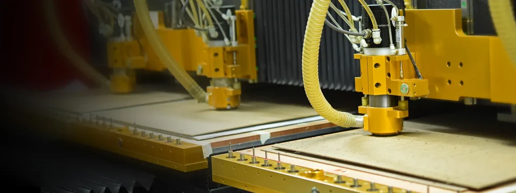
Shenzhen Jingpeng Electronics | PCB Manufacturing and Engineering Review
Layers 2–32
Range of Multilayer Boards
0.4–4.0 mm
Sheet Thickness Range
1st–3rd order
HDI Structure
Parameter applicability depends on the board material, number of layers, copper thickness, dimensions, and via structure; the listed limit values do not imply that all can be achieved simultaneously.
01 / Product Specifications
First, confirm the number of layers, board thickness, and finished dimensions.
- Number of Layers and HDI
- Layers 2–32; HDI supports 1st–3rd-order structures; specific mechanical via and laser-drilled blind via configurations are subject to stack-up review.
- Thickness of the finished panel
- 0.4–4.0 mm; the applicable board thickness depends on the number of layers and the structure.
- Sheet Thickness Tolerance
- Sheet thickness ≥ 1.0 mm: ±10%; sheet thickness < 1.0 mm: ±0.1 mm.
- Maximum Finished Product Dimensions
- Single-sided, double-sided, and 4-layer boards: 520 × 600 mm; boards with ≥6 layers: 400 × 500 mm.
- Minimum Size · OSP
- 80 × 50 mm.
- Minimum Size · Non-OSP
- The original specifications list two sizes: 50 × 50 mm and 10 × 10 mm; the applicable area requirements and panel layout must be confirmed by the project team.
For small-sized panels, irregularly shaped panels, and special panel assemblies, please provide the panel dimensions and assembly drawings; do not judge manufacturability based solely on individual dimensions.
02 / Drilling and Tolerances
Verify the hole diameter, hole location, and hole structure separately
- Machined Round Hole
- Hole diameter: 0.15–6.35 mm; for diameters greater than 6.35 mm, a hole-enlarging process may be used; the specific procedure shall be confirmed in accordance with the documentation.
- Laser-Cut Round Holes
- Pore size: 0.075–0.15 mm; for larger pore sizes, evaluate whether it is appropriate to switch to mechanical drilling.
- Groove Hole
- Metallized slot holes: ≥0.50 mm; non-metallized slot holes: ≥0.80 mm.
- Hole Tolerances
- ±0.075 mm.
- PTH Hole Size Tolerance
- Standard holes: ±0.075 mm; crimp holes: ±0.05 mm.
- Other Hole Diameter Tolerances
- NPTH: ±0.05 mm; Slot: ±0.1 mm.
- Thickness-to-Diameter Ratio
- 10:1 (ratio of plate thickness to hole diameter); the applicability to specific structures is subject to review.
- Half-hole
- Diameter ≥ 0.5 mm; spacing ≥ 0.9 mm. Please specify the basis for measuring the spacing in the drawing.
Please distinguish between the drilling diameter and the finished hole diameter, and specify PTH, NPTH, crimp holes, and special tolerances. The same parameters cannot be directly applied to different hole types.
03 / Sheets and Properties
Specify the complete grade, then verify the material properties.
Material Grades and Brands
Grade A materials. The current range of materials includes Shengyi, Kingboard, Rogers, Panasonic, Isola, Ventec, AGC, Arlon, and TUC; specific models and availability are subject to project confirmation.
Heat Resistance and Electrical Specifications
The original specifications list Tg 130°C/150°C/170°C, CTI ≥175 V, and breakdown voltage ≥4000 V. Since specifications may vary depending on the material grade and test conditions, please refer to the data sheet for the selected material.
Flame Retardancy Ratings and Material Selection
The original specifications list UL 94 V-0. The project must confirm the grade of the corresponding material and the supporting documentation; requirements for high frequency, high reliability, or special environmental conditions must be specified separately.
Brand names cannot be used as substitutes for material grades. Please also provide the dielectric thickness, copper thickness, number of layers, and key performance requirements; any material substitutions must be approved by the design team.
04 / Special Processes
Selecting a Process Based on Structural Requirements
HDI and Through-Hole
HDI 1–3-layer, through-hole (POFV), and blind-hole plating. Please provide the stack-up, hole specifications, and plating requirements to confirm the process combination.
Half-Hole and Metal Edging
Used for edge connections or specific structural designs. Please specify the positions of the half-holes, the edge-wrapping range, and related dimensions, and evaluate the machining process in conjunction with the plate and frame.
Process Edges and Panel Joining
Processing allowance: ≥3 mm. Please specify the panel layout, spacing between panels, location holes, and machining requirements; confirm the layout in conjunction with subsequent assembly.
Precision Drilling and Milling and Cavity Structures
Controlled-Depth Drilling
Deep Trough Control
Irregular-shaped holes
Stepped Trough
Board-to-Board Connections and Passive Functions in Inner Layers
Metal edging
PCB Buried Resistors
Buried-Capacitor PCB
Local Heat Dissipation and Thermoelectric Structures
Copper-Embedded PCB
Thermal-Electric Separation PCB
05 / Select by Product
Learn more about PCB solutions for your project
High-Frequency PCBs
Focus on materials, RF paths, and stack consistency, and clarify the manufacturing requirements for key networks.
View DetailsThick-Copper PCB
Conduct a process review taking into account current-carrying capacity, heat dissipation, finished copper thickness, and pattern requirements.
View DetailsMetal-Cored PCB
Evaluate heat dissipation solutions based on the insulation layer, the metal substrate, and structural requirements.
View DetailsFlexible PCB
Define the material and structural requirements based on the space available for bending, joining, and assembly.
View DetailsRigid-Flex PCB
Define the rigid zone, flexible zone, transition zone, and the overall laminate.
View DetailsRadar PCB
Identify key processes related to RF trace routing, antenna areas, and material structures.
View Details06 / Project Review and Request for Quotation
Convert parameters into actionable production requirements
01 · Submit all required documents
Gerber or ODB++ files, drill files, mechanical drawings, layer stacks, and material specifications. Please ensure that all files correspond to the same design version.
02 · Highlight Key Requirements
Specify impedance, trace width and spacing, copper thickness, surface treatment, and inspection requirements; please confirm any parameters not listed on this page separately in the documentation.
03 · Confirming the Quote and Delivery
Please provide the quantity, desired delivery date, panel consolidation details, and reporting requirements. Once the engineering review has confirmed the process combination, we will finalize the quote and production schedule.
Is it possible to design while simultaneously meeting all minimum or maximum parameters?
You cannot make that determination directly. The number of layers, board thickness, hole diameter, material, and special processes are all interrelated; the actual manufacturability range should be confirmed based on the complete documentation.
Why aren't the line widths, line spacings, copper thickness, and impedance tolerances listed in a single table on this page?
These parameters must be determined based on the material, copper thickness, number of layers, and pattern structure. Please provide the target values and design documents so that our engineering review team can propose a corresponding solution.
Can items that exceed the page parameters be evaluated?
You may submit documentation outlining the target requirements, and the engineering team will determine whether they are feasible and whether design adjustments are necessary. The parameters on this page do not replace the process validation required for a specific project.
Shenzhen Jingpeng Electronics
Get your files ready and start your PCB project
Provide design documentation and key parameters to ensure a smoother transition between engineering reviews, quoting, and prototyping.
