

PCB layout (Printed Circuit Board Layout), also known as PCB layout or PCB design, is a critical step in the manufacturing process of electronic products. It involves the proper arrangement and connection of electronic components according to a predetermined circuit diagram to create a fully functional, stable printed circuit board (PCB). PCB layout is not merely about placing components; it also involves various aspects such as trace routing, thermal management, and electromagnetic compatibility.
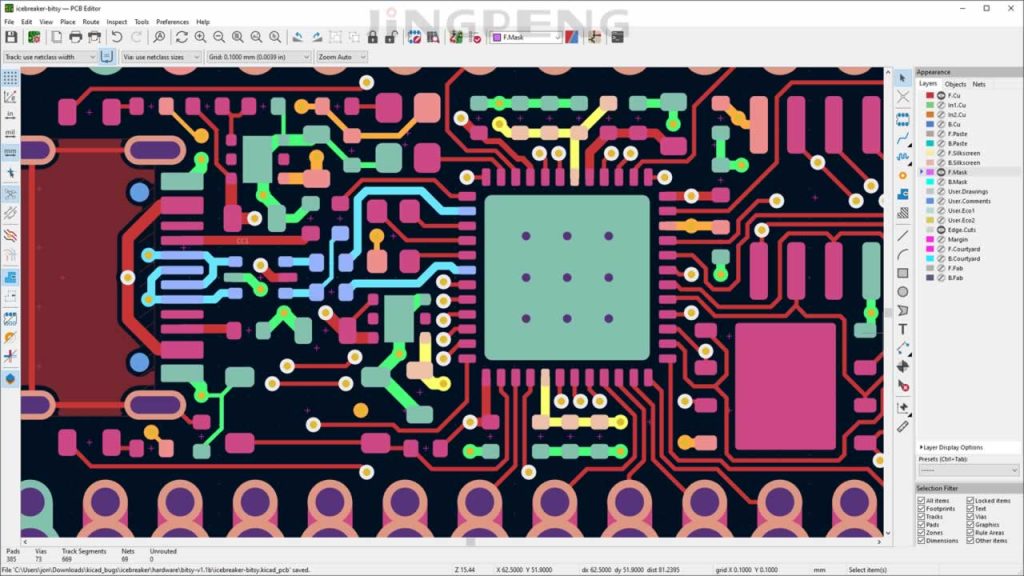
The Importance of PCB Layout
PCB layout plays a crucial role in the entire electronic product design and manufacturing process, as it directly affects the performance, stability, and reliability of the circuit. A well-designed PCB layout offers the following key benefits:
- Signal Integrity: A well-designed layout can minimize signal path length, reduce signal transmission delay and loss, and thereby improve signal integrity and stability.
- Electromagnetic Compatibility: PCB layout can affect electromagnetic radiation and interference between sensitive components. A well-designed layout can reduce electromagnetic interference and ensure that different components function properly.
- Heat Dissipation Performance: A well-designed PCB layout can place components that generate a significant amount of heat in areas with good heat dissipation, which helps improve the overall heat dissipation of the circuit board and prevents component damage due to overheating.
- Easy to maintain: If the PCB is laid out properly, it can make the connections between components clearer, making it easier for maintenance personnel to troubleshoot and repair the board.
Steps for PCB Layout
A successful PCB layout requires the following steps:
- Circuit Analysis: First, we need to analyze the circuit to understand the connections between the various components and the signal transmission requirements.
- Component Placement: Based on the circuit diagram, place each component on the PCB according to specific guidelines, taking into account factors such as heat dissipation, signal paths, and layout compactness.
- Wiring Design: Design the wiring layout to ensure stable and reliable signal transmission and prevent signal crosstalk and electromagnetic interference.
- Ground Plane and Power Plane: Designing ground planes and power planes helps reduce interference from ground and power lines and improves electromagnetic compatibility.
- Heat Dissipation Design: Place components that generate a significant amount of heat in locations with good heat dissipation, and consider using heat sinks or heat spreaders to dissipate the heat.
- Design Review: Conduct a design review of the PCB layout to ensure there are no omissions or errors, thereby guaranteeing the stability and performance of the circuit.
- Simulation and Testing: The layout can be simulated using simulation software to verify the circuit's performance. At the same time, actual testing is also required to ensure that the circuit board functions properly.
In the manufacturing process of modern electronic products, PCB layout is a critical step in ensuring circuit performance and stability. Through proper component placement, trace routing, and thermal design, the reliability and performance of the circuit can be enhanced, thereby ensuring the normal operation of electronic products. Therefore, it is essential to give full consideration to the layout phase in PCB design, as it directly impacts the quality and performance of the final product.
