Warpage * | Review Based on Package Dimensions and Customer Specifications | Large-size FCBGA requires specialized simulation and tooling evaluation |
Solder Ball Coplanarity * | Verify based on packaging specifications and measurement methods | Classified by package size; measured according to JEDEC methods |
Minimum BGA Ball Pitch * | Specialized Review of Pad/Ball Structures | Subject to the combined constraints of solder ball size and stencil capacity |
Minimum Inter-Key Spacing * | Specialized Review of Bonding Methods and Patterns | Suitable for wire-bond carrier boards |
| Sheet Thickness Tolerance | ± 10% / Thin sheet ± 0.03 mm | For values below 0.2 mm, control based on absolute values |
| Dimensional Tolerances | ± 0.10 mm Edge Milling / ± 0.05 mm Laser | Laser cutting is recommended for irregular shapes and high-precision contours |
| Solder Mask Alignment Accuracy | ± 25 μm | The precision of window cutting directly affects the yield rate of ball planting. |
ENEPIG Coating Thickness * | Confirmed in accordance with the customer's plating specifications | Can be adjusted according to customer specifications; a film thickness report is included with the shipment. |
ENIG Coating Thickness * | Confirmed in accordance with the customer's plating specifications | Lower cost than ENEPIG; suitable for applications that do not require wire bonding |
Key Parameters of the Substrate * | Verify based on the specified material grade / datasheet | The ABF system uses low loss values; high-frequency scenarios are subject to separate discussion. |
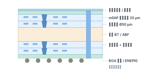
| Layered Structure | C+2+2+C / 2+2+2 / 3+2+3 | Designed according to the number of layers, wiring density, and warpage requirements |
| Delivery Format | Single chip / strip / array | Determined based on the subsequent packaging process; vacuum anti-static packaging |
| Reliability Testing | TCT / HAST / HTS / PCT / Reflow Soldering Simulation | Internal reports can be provided; third-party reports will be arranged separately. |