

Vias (short for ”Vertical Interconnect Access”) are one of the key components of multilayer PCBs and play a crucial role in the design and manufacturing of electronic devices. This article will take an in-depth look at the structure, classification, and design recommendations for vias, with a particular focus on how the aspect ratio affects via performance and cost.
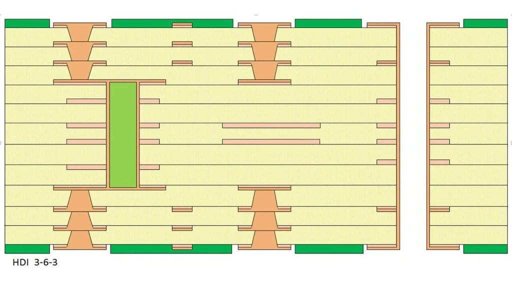
The Structure of a Via
A via consists of three main parts: the drill hole, the pad area, and the POWER layer isolation zone. The drill hole is located in the center and is used to connect the copper foil layers of the circuit board, ensuring the transmission of signals and power. The pad area is the region surrounding the drill hole and is used for soldering and connecting components. The power layer isolation zone is used to block interference between different power layers.
Classification of Via Holes
Vias are generally classified into three types: blind vias, buried vias, and through-hole vias.
- Blind vias: Located on the top and bottom surfaces of a printed circuit board, they have a certain depth and are used to connect surface-level traces to internal traces.
- Through-hole: Located within the inner layers of a circuit board, invisible from the surface, and used to connect internal circuits.
- Through-hole: A hole that passes through the entire circuit board, commonly used for positioning and mounting components.
Design Recommendations for Via Holes
At high speeds and high densities (HDI) In PCB design, the size of vias is particularly important. Designers typically prefer vias to be as small as possible to save routing space and reduce parasitic capacitance. However, adjusting the via aspect ratio requires a comprehensive consideration of factors such as cost and manufacturing processes.
The recommendations are as follows:
- Calculate the aspect ratio appropriately to ensure the stability and reliability of the vias.
- For high-speed signal lines, consider using smaller via diameters to reduce parasitic capacitance and improve signal transmission performance.
- For signal lines with special requirements, such as power lines and ground lines, increase the hole diameter appropriately to improve current-carrying capacity.
- Pay attention to the minimum hole diameter to avoid off-center drilling and uneven plating.
- Avoid drilling holes deeper than six times the diameter of the drill bit to ensure an even copper plating.
The Effect of the Pore Size Ratio
The via aspect ratio is a critical parameter in via design. It is the ratio of the via diameter to the diameter of the pad area surrounding the via. An increased via-to-pad ratio can result in an unstable via connection, potentially causing signal interference or an unstable power supply. However, an excessively small via-to-pad ratio increases manufacturing costs and is also subject to limitations imposed by manufacturing processes such as drilling and plating.
Therefore, during the design process, it is necessary to select an appropriate aspect ratio to balance performance and cost. Professional electronic engineers typically plan and adjust accordingly based on specific requirements to ensure excellent performance and reliability of the vias.
Vias, as critical connection elements in electronic devices, ensure the stable operation of circuit boards and reliable signal transmission. Proper via design can enhance PCB performance and reliability; however, it is also important to consider the impact of the aspect ratio on via cost and performance.
We hope this article has provided you with some useful guidance on understanding vias and optimizing your designs. If you have any further questions about vias, please feel free to contact Jingpeng at any time!
