

Communications and Electronics PCBs | From RF Links to Materials and Geometric Tolerances
The performance of antennas, RF front-ends, and communication modules depends on the combined effects of the frequency band, transmission structure, copper foil, dielectric materials, and connection transitions. This page focuses on the evaluation of loss, phase, and impedance in RF PCBs; for high-speed digital switching and server interconnects, see the Digital Communications section.

Exhibits Related to Communications and Electronics | The specific scope of application will be determined on a project-by-project basis.
First, distinguish between feedlines, antennas, and RF front-ends
PCBs in telecommunications equipment serve different functions, and the geometric and manufacturing parameters of interest vary accordingly.
Antennas and Feed Networks
Phase consistency, feedline geometry, and the dielectric environment in the antenna region are key inputs. Enclosures, mounting structures, and coverings can also alter the actual conditions; manufacturing documents should clearly distinguish between the antenna region and the general circuit region.
Filtering, Coupling, and Matching Structures
Critical spacing, line width, copper thickness, and etch morphology all affect the structural response; key control areas and design tolerances must be specified—it is not sufficient to provide only general line width requirements for the entire board.
Power Amplification and RF Front End
Since both RF loss and heat dissipation from the components must be considered, the connectors, ground vias, and heat sink mounting surfaces must be evaluated together. Changes in copper thickness and thermal design may also alter the original transmission line geometry.
Wireless Access and Communication Control
When RF, clock, digital control, and power components are on the same board, first identify the coupling paths and reference planes; clearly delineate the specific requirements for the RF area, and design the other areas according to their corresponding electrical functions.
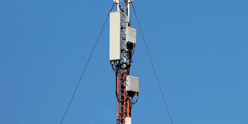

Images related to applications and manufacturing are used solely to illustrate the scenarios.
Materials account for only a portion of the loss budget.
Establish comparisons based on the same frequency, length, structure, and measurement methods, and avoid directly combining values from different data tables.
Media: Comparison Methods and Frequency Conditions
Dk affects the electrical length and impedance of the transmission structure, while Df is related to dielectric loss. The data source, frequency, and test methods should be verified, and the design model must be compatible with the selected materials and structure.
Conductor: Copper Foil and Final Product Geometry
The surface roughness of the copper foil, the copper thickness, and the line profile after etching all affect high-frequency performance. When specifying copper foil, it is also important to verify processability and adhesion requirements; the performance of the entire board cannot be judged based solely on a single roughness rating.
Transition: Connectors and Layer-Change Areas
Connector pads, vias, and reflow connections can create local discontinuities. Transition structures should be included in the model or verification, rather than attributing all insertion loss to the substrate.
Overlay and Surface: Ensuring Consistency Between Design and Physical Object
Solder mask, surface treatment, shielding, and adjacent structures can alter the transmission environment. Indicate which areas are covered and which are excluded, and provide feedback on the changes to the design team for confirmation.
Engineering Example: Why Might Two Feeder Lines of Equal Length Still Have Different Phases?
This example is intended to illustrate the evaluation method and does not represent the performance data of any specific antenna product.
Equal length does not mean the same electrical length
If two lines use different reference planes, have partial overlaps, or include transition structures, they may have different propagation conditions even if their CAD lengths are the same. Check the entire path first, rather than directly adding serpentine line compensation.
First, make sure the conditions for comparison are consistent.
Verify layer positions, dielectric thicknesses, trace widths, grounding, and connectors; compare results on the same reference plane and within the same frequency range. If necessary, design a dedicated test structure to isolate the effects of long traces from those of connection transitions.
To apply the changes, you must return to the manufacturing file.
If changes are made to the dielectric, copper foil, or coverage area, re-verify the impedance and critical dimensions, and retain the approved version. Substituting materials without design verification may render the original electrical model invalid.
RF Verification: Define the Reference Plane First, Then Discuss the Results
The scope of the sample testing should be clearly defined; otherwise, the data in different reports will not be directly comparable.
01
01|Freezing the Test Subject
Define the frequency range, ports, cable length, and transmission structure, and mark the locations of the test connectors or probes. Confirm whether you are testing material samples, bare board structures, or fully assembled channels.
02
02|Alignment Measurement Methods
When using network analysis measurements, agree on the calibration, reference plane, and whether to perform de-embedding; impedance testing and RF S-parameter testing are not equivalent forms of evidence and should not be used interchangeably in acceptance conclusions.
03
03|Linking Physical Items to Reports
Keep records of prototype numbers, lamination, material lots, and critical dimensions. When dealing with anomalies, first isolate the effects of the instrument, fixtures, connections, and board structure, and then determine which process parameters need to be modified.
Selecting Materials and Fabrication Processes for RF Structures
Refer to the following panel types and process inlets to further verify the specific structure, drawings, and acceptance requirements.
High-Frequency PCBs
For high-frequency PCBs, the frequency band, transmission line type, dielectric thickness, and copper foil must all be specified; simply specifying “low loss” is insufficient to define the actual stack-up and geometry.
Radar PCB
For radar and array antennas, the review should focus on feed phase, key geometric parameters, and material consistency; the frequency band, antenna coverage area, and installation environment must be specified separately; specifications cannot be defined solely by the name of the high-frequency board.
HDI PCB
The high-density control section can evaluate HDI, but RF trace layering, via structures, and reference planes must be modeled separately; microvias do not automatically result in lower loss.
PCB Materials
The materials sheet is used to compare grade specifications; formal drawings should specify the core material, bonding material, thickness, and copper foil type. The methods and conditions used to test Dk must be verified against the Dk values used in the design. For mixed-pressure applications, the dimensional stability of the material combinations must also be evaluated.
Thick-Copper PCB
The power supply section of communication equipment can be evaluated in terms of copper thickness and current connections; however, its manufacturing requirements should be specified separately from those of the RF section. Increasing the copper thickness may alter the etching clearance and the overall stack-up, requiring a comprehensive review.
PCBA Testing
During the assembly verification phase, check the RF connectors, shielding, ground solder joints, and test access points. The measured channel results also include assembly-related effects; therefore, measurement boundaries must be defined for both the bare board and the fully assembled board.
RF schematics should be accompanied by a separate bill of materials.
This helps manufacturing engineers identify areas that require close attention and enables test engineers to know how to compare samples.
Materials and Layer Structures
Complete part number, core board/bonding layer, dielectric thickness, copper foil type, finished copper thickness, and mixed-pressure requirements.
Key Geometry
RF network identifiers, trace width and spacing, reference planes, via structures, coverage and surface treatment areas, and connector mounting references.
Acceptance Criteria
Test configuration, frequency range, reference plane, targets, and tolerances; whether dimensional reports, impedance measurements, or other agreed-upon measurement records are required.
Communications and Electronics PCBs: Answers to Specific Questions
Are panels from the same Rogers brand directly interchangeable?
It is necessary to compare specific part numbers, substrate thicknesses, copper foil, bonding systems, and electrical models. The fact that the brands are the same does not mean that the transmission structures or processing conditions are equivalent.
Does passing the impedance test mean that the RF loss is within specifications?
No. Impedance describes different characteristics related to loss; RF acceptance testing must also define the frequency, structure, and measurement methods in accordance with project requirements.
Should the solder mask be completely removed from all RF traces?
This must be consistent with the design model, protection, and assembly requirements. Implement only after clearly specifying the target area; do not apply local optimization methods to the entire board.
The reference materials are intended to help you understand the relevant technical principles; specific parameters and applicable conditions are subject to the project documentation and the corresponding device and material specifications.
Rogers: Understanding Material Dk and Design DkRogers: RF Materials and Transmission Line Simulation ToolsHigh-Speed Digital Links: Explore Data Communication ApplicationsInitiate the RF manufacturing review using frequency bands, stacking, and critical paths
Shenzhen Jingpeng Electronics | Please submit complete specifications, including part numbers, frequency bands, transmission structures, copper foil, and key tolerances. If measurement coordination is required, please also provide reference surfaces, test structures, and acceptance criteria.
