

I. Basic Understanding of PCB Stencils
1.1 Definitions
A PCB stencil is essentially a thin sheet made of stainless steel or another alloy material, with a series of small holes precisely cut into it to correspond one-to-one with the component layout on the PCB, laying the foundation for subsequent solder paste printing, component placement, and soldering.
Specifically, PCBs contain a large number of surface-mount ICs, resistors, capacitors, and other components. During the soldering process, a reflow soldering machine is used for automated soldering, and before soldering, solder paste must be applied to the pads of the surface-mount components. The primary function of the stencil is to ensure the precise application of the solder paste.
During the solder paste application process, the circuit board is placed beneath the stencil, and the solder paste is dispensed onto the stencil. After being spread evenly with a squeegee, the solder paste flows through the stencil apertures onto the corresponding pads on the PCB. Following component placement, the board is fed into the reflow oven to complete the soldering process.
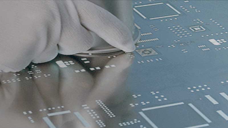
1.2 Key Roles
The primary function of a PCB stencil is to ensure that solder paste (or red glue) is transferred evenly and precisely to the designated pad locations on the PCB, thereby ensuring the soldering quality and reliability of surface-mount components.
Specifically, this is reflected in:
- Precise positioning ensures that, through accurate alignment with the PCB, the solder paste is applied only to the target pads;
- Apply the solder paste evenly to avoid using too much or too little;
- Improve efficiency and adapt to automated production lines for SMT assembly to achieve high-volume, efficient solder paste printing operations.
II. Manufacturing Process for PCB Stencils
The manufacture of steel mesh is a precision process centered on “accurately matching PCB pads,” involving various technologies such as CAD design, laser cutting, and electrochemical etching. The specific process is as follows:
First, engineers use CAD software to create precise stencil drawings based on the component layout and design requirements of the PCB;
Next, the drawings are converted into a machine-readable format, and holes are precisely cut into the steel plates using specific machining processes;
Finally, ensure that the position, size, and shape of the holes correspond exactly to the pads on the PCB to guarantee the accuracy of solder paste printing.
2.1 Common Types of Manufacturing Processes
Currently, the two main methods for manufacturing steel mesh are laser cutting and electrochemical etching. Among these, the laser cutting process has become the more widely used method due to its significant advantages. In addition, specialized manufacturing processes for stepped steel mesh have been developed to meet specific requirements.
(1) Laser Cutting Process (Laser-Cut Steel Mesh)
This process relies primarily on machine processing; staff members need only design the apertures and import and export the files, after which the laser cutter will engrave the steel mesh based on the files. The mesh is then polished to improve solderability.
Its key strengths include:
- High precision, with positional and dimensional accuracy errors of only 3 µm for holes in the template;
- Short processing cycles, driven by data and requiring no complex processes;
- Consistent quality that does not rely on complex chemical formulations or process parameter controls;
- The hole walls are smooth (roughness < 3 µm), and the beam’s focusing characteristics allow the hole to be formed with a taper that is narrower at the top and wider at the bottom, facilitating the release of solder paste and enabling precise control over the volume and shape of the solder paste applied to the pad;
- It is environmentally friendly, requires no chemical solutions, and causes no environmental pollution. The downside is that it is relatively expensive.
(2) Electrochemical Corrosion Process
One of the traditional methods for making steel screens involves etching holes in steel plates using chemical solutions.
Its advantages include lower costs, making it suitable for mass production of simple designs; however, it has drawbacks such as lower precision, higher surface roughness of the holes, longer processing cycles, and the need to dispose of chemical waste, which can cause environmental pollution. As a result, it is gradually being replaced by laser cutting processes.
(3) Manufacturing Process for Stepped Steel Mesh
The core feature of a stepped steel mesh is the creation of two or more different thicknesses on a single mesh plate to meet the varying solder paste requirements of different components. This design accommodates scenarios where electronic components of varying sizes are present on the same side of a circuit board, ensuring soldering quality. Depending on the required thickness adjustments, these can be classified into two types: STEP-UP (local thickening) and STEP-DOWN (local thinning). During manufacturing, the specific location of the stepped structure must be determined based on the specific process sequence (whether solder paste or red glue is applied first).
III. Classification and Specifications of PCB Stencils
3.1 Common Classifications
Based on factors such as application and manufacturing process, common PCB stencils can be classified into the following categories:
(1) Solder Paste Stencil
This is the most commonly used type of stencil in SMT assembly factories, and its primary purpose is to apply solder paste. During manufacturing, the aperture size must be adjusted according to actual process requirements. For components that require a larger amount of solder paste, this is typically achieved by increasing the size of the pads and the stencil apertures, rather than increasing the stencil thickness. This prevents manufacturing defects—such as short circuits in high-density ICs—that can result from excessive stencil thickness.
Its thickness is generally 0.05–0.15 mm.
(2) Red-rubber-coated steel mesh
The hole is typically located between the two pads of the component. Its primary purpose is to transfer red adhesive to the PCB via dispensing, thereby temporarily securing the component in place. Subsequently, through-hole components must be inserted so that the entire assembly can undergo wave soldering.
With the trend toward miniaturization of electronic components, this type of steel stencil is gradually being phased out of mainstream SMT assembly processes. Currently, it is used only on boards containing high-power components and chip components, such as power supply boards, and its thickness typically ranges from 0.18 to 0.3 mm.
(3) Dual-process steel mesh
Designed for applications where a single PCB requires both solder paste and red glue application, this solution consists of two stencils (one standard laser-cut stencil and one stepped stencil).

The design must follow the principle of process sequence:
If solder paste is applied first, the solder paste stencil should be made as a standard laser-cut stencil, and the red glue stencil should be made as a stepped stencil;
If the red adhesive is applied first, the red adhesive stencil should be made as a standard laser-cut stencil, and the solder paste stencil should be made as a stepped stencil.
(4) Laser-cut steel stencil
Steel stencils produced using laser cutting technology are currently the most common type of steel stencil. They offer advantages such as high precision, fast processing, and consistent quality, making them suitable for the vast majority of PCB surface-mount assembly applications.
3.2 Common Specifications
(1) Dimensions and Specifications
Common steel mesh sizes include 37×47 cm, 42*52 cm, 55*65 cm, 60*65 cm, 65*65 cm, 73.6*73.6 cm, etc.
Generally, a fully automatic solder paste printer on an SMT assembly production line must be configured with at least 42*A 52-cm stencil; if the customer does not have specific requirements for the stencil, it can be selected based on the PCB dimensions—as long as the PCB dimensions are smaller than the stencil’s effective area, for example, 8 ×For 20-cm boards, you can choose 37*47 cm steel mesh; for double-sided surface-mount boards, double the single-sided dimensions (e.g., 8 ×20 cm double-sided patch, 16*(calculated at 20 cm), you can still choose 37*47-cm SMT laser-cut stencil.
(2) Thickness Specifications
Common thickness specifications for steel stencils include 0.8 mm, 1.0 mm, 1.2 mm, 0.13 mm, 0.15 mm, 0.18 mm, 0.2 mm, 0.25 mm, and 0.3 mm, among others, with solder paste stencils typically ranging from 0.05 to 0.15 mm in thickness, and red adhesive stencils generally ranging from 0.18 to 0.3 mm.
IV. How to Select a PCB Stencil
Selecting the appropriate steel mesh is key to ensuring the quality of SMT assembly. This requires a comprehensive assessment of core factors such as material, thickness, aperture size, and manufacturing processes, while also taking into account the requirements of the actual application scenario.
4.1 Key Selection Factors
(1) Material Selection
Wire mesh is primarily made of stainless steel or other alloy materials. Since different materials vary in hardness, corrosion resistance, and wear resistance, the choice should be based on the specific application and frequency of use: For routine mass production and high-frequency use, stainless steel is recommended due to its superior wear resistance and stability; For special environments (such as those that are humid or contain corrosive gases) or scenarios with low usage frequency, an appropriate alloy material can be selected based on the cost budget.
(2) Selecting Thickness and Hole Size
The thickness of the steel mesh and the size of the apertures directly affect the solder paste printing results, requiring a balance between printing precision and operational stability: Thinner steel mesh and smaller apertures provide finer printing results, making them suitable for processing small components (such as high-density ICs), but they increase the risk of aperture clogging; Thicker stencils with larger apertures are suitable for processing large components that require a greater amount of solder paste, but care must be taken to avoid issues such as short circuits caused by excessive thickness.
When making an actual selection, specific parameters must be determined based on the component type and pad size; if necessary, adjust the aperture size instead of the thickness.
(3) Selection of Manufacturing Processes
Different manufacturing processes directly affect the precision, durability, and cost of steel stencils, so the choice should be based on processing requirements: For standard manufacturing scenarios, applications with high precision requirements (such as the placement of small components), and when the budget allows, laser cutting should be the preferred method; For applications with lower precision requirements, simple stencil designs, and limited budgets, electrochemical etching is a suitable option; if a single-sided PCB contains components requiring different amounts of solder paste, a stepped stencil manufacturing process should be selected; and if both solder paste and red glue printing need to be completed simultaneously, a dual-process stencil should be chosen.
4.2 Practical Recommendations
Standard laser-cut stencils can meet the processing requirements for the vast majority of products. If special types of stencils are required (such as stepped stencils or dual-process stencils), SMT manufacturers should communicate with customers promptly to confirm the details and avoid any impact on placement yield due to stencil incompatibility.
At the same time, stencil prices range from tens to hundreds, and their quality is influenced by factors such as materials, design, and manufacturing processes. We recommend prioritizing certified, high-quality stencils—high-quality stencils provide better solder wetting, enhance placement accuracy and aesthetics, and significantly improve product yield. This helps avoid product quality issues caused by low-cost, substandard stencils, which could otherwise result in even greater losses.
V. Use and Maintenance of PCB Stencils
5.1 Proper Usage
The use of steel meshes requires following the appropriate operating procedures based on their type; the key is to ensure precise alignment between the steel mesh and the PCB:
(1) Steps for Using a Solder Paste Stencil
First, align the solder paste stencil with the PCB to ensure that all holes are perfectly aligned with their corresponding pads;
Step 2: Apply solder paste onto the stencil and use a squeegee to spread it evenly, allowing the solder paste to pass through the apertures and cover the PCB pads;
Step 3: Place the surface-mount components precisely on the pads coated with solder paste, ensuring that the components are aligned with the pads;
Step 4: Feed the PCB into the reflow oven to heat it, causing the solder paste to cure, thereby completing the soldering process.
(2) Instructions for Using the Red Rubber Net
Step 1: Align the red silicone mesh with the PCB. Make sure the holes line up with the center of the components on the PCB, avoiding the pads;
Step 2: Use a dispensing machine to apply red adhesive through the holes in the steel mesh onto the PCB;
Step 3: Place the surface-mount components on the red adhesive, ensuring they are securely attached;
Step 4: Heat the PCB to cure the red adhesive;
Step 5: Insert the components and place the PCB into the solder pot to complete the soldering.
5.2 Key Maintenance and Care Points
Steel screens require regular cleaning and maintenance during use. The primary purpose is to remove solder paste and impurities that clog the apertures, maintain optimal performance, and extend their service life.
Specific points include:
First, clean it regularly. After each use or whenever the nozzles become clogged, clean them promptly with a specialized cleaning agent to prevent solder paste residue from drying and becoming difficult to remove;
Second, store the steel mesh properly. After washing and drying, lay it flat in a dry, clean environment to prevent deformation caused by crushing or impact, and keep it away from damp and corrosive environments;
Third, conduct regular inspections. Before use, check the steel mesh for deformation, holes, wear, blockages, or other issues, and repair or replace it promptly if any abnormalities are found;
Fourth, choose appropriate cleaning agents and maintenance tools, and avoid using highly corrosive cleaners to prevent damage to the steel mesh.
VI. PCB Stencil-Related Documents and Frequently Asked Questions
6.1 Notes on Steel Mesh Files
The stencil file in PCB design is the key reference for stencil fabrication, ensuring that the stencil apertures precisely align with the PCB pads and component locations.
After completing a design using PCB design tools such as Protel, you can export Gerber files, which include GTP (top-layer stencil file), GBP (bottom-layer stencil file), and several files named SMT. These files contain key information such as the location, size, and shape of the stencil apertures, and serve as the core data for stencil fabrication.
6.2 Frequently Asked Questions
What is the difference between a PCB stencil and a PCB board?
A PCB stencil is a steel plate with precisely cut openings; its primary purpose is to provide support and positioning for the application of solder paste (or red glue) onto the pads of a PCB. A PCB, or printed circuit board, is a board populated with electronic components and interconnecting circuits, serving as the substrate for mounting and connecting electronic components.
The two are completely different in terms of function, material, and purpose; they serve as complementary tools and the core components in SMT assembly.
How does the quality of a PCB stencil affect soldering quality?
The quality of a PCB stencil directly determines the accuracy and uniformity of the soldering process: A high-quality stencil ensures uniform solder paste application and precise positioning, thereby improving the soldering quality and reliability of surface-mount components; If the stencil is poorly manufactured (e.g., misaligned apertures, inaccurate dimensions, or rough aperture walls) or used improperly (e.g., incorrect positioning or failure to promptly clean clogs), it can lead to uneven solder paste application and and misaligned component placement. In severe cases, this can lead to soldering defects, short circuits, and other failures, directly affecting the performance and reliability of electronic components.
Why are two different types of PCB stencils (solder paste stencils and red glue stencils) needed?
The key difference between solder paste stencils and red glue stencils lies in the different surface-mount processes they are used for: Solder paste stencils are used in the solder paste printing process, where components are soldered and secured to the PCB through the thermal curing of the solder paste; Adhesive stencils are used in the adhesive-fixation process, in which components are first temporarily secured to the PCB with adhesive, and then soldered via wave soldering.
The design of both (such as the location of the holes and thickness) and their intended uses are tailored to different process requirements; therefore, they must be used appropriately.
The formatting has been fully optimized to comply with pure HTML standards. Would you like me to review it to make sure there are no missing or unnecessary attributes, or should I organize the optimized content into text snippets so you can copy them directly into WordPress?
