Radio FrequencyThe design of the RF section layout is critical in electronic products, particularly in mobile phone manufacturing. Ensuring that the RF section is laid out properly and accurately can significantly impact product performance and reliability. This article will explore the key principles of RF section layout to help you better plan and design mobile phone PCBs, ensuring smooth signal transmission and optimal performance.
1. Why does RF layout require a separate set of rules?
Digital circuit layout focuses on timing and signal integrity, while RF layout focuses onPower Transmission, Noise Isolation, and Parasitic Parameters. The two have different focuses and different rules. The three characteristics of the RF link dictate that it must be treated differently:
- Extremely wide dynamic range: The transmitter PA can output up to +30 dBm (1 W), while the receiver must detect signals as low as −100 dBm—a difference of more than 130 dB. Even the slightest coupling can overwhelm the desired signal.
- Susceptible to parasites: A 1 nH parasitic inductance on an RF trace is equivalent to an impedance of approximately 12 Ω at 2 GHz, which is sufficient to alter the matching network; a 1 pF parasitic capacitance is equivalent to approximately 80 Ω at the same frequency. Therefore, RF traces are not simply a matter of “just connecting them.”
- Nonlinearity: A PA is a highly nonlinear device whose output contains a rich spectrum of harmonics; these harmonics are coupled back into the receive chain via the power supply or through the air, causing self-oscillation and spurious emissions.
Once you understand these three points, all the other rules—such as marking the area, creating a buffer zone, using a heavy-duty power cord, and maintaining a clear space—will follow naturally.
2. Device Packaging Inspection
Before designing an RF layout, you must first carefully inspect the component packages on the main board. This is especially important for projects using new materials; in such cases, you must carefully inspect the PCB packages in strict accordance with the specifications to avoid potential issues.
The Three Most Common Sources of Errors in RF Device Packaging:
- Ground pad on the bottom of the device: Components such as PA, FEM, and filters typically have exposed heat sink/ground pads on their bottoms. It is essential to cut a window in the package and fill it with ground vias according to the specifications; failure to do so will directly result in reduced gain and inadequate heat dissipation.
- Pin Numbers and Orientation: The pin definitions for multi-port devices such as FEM and ASM are complex; drawing them in the wrong orientation will cause the inputs and outputs to be swapped, rendering the board unusable.
- Source of Package Dimensions: Be sure to create the library using the optimal dimensions (Nominal) from the latest version of the device datasheet, rather than the maximum values (Max). Using the maximum values will result in pads that are too large, which will affect high-frequency performance.
3. Component Layout
When performing stacking, careful consideration must be given to the layout of structural elements and key components. These components may include I/O connectors, SIM card slots, battery connectors, T-card slots, cameras, speakers, receivers, RF sections, baseband sections, GSM antennas, Bluetooth antennas, and mobile TV antennas, among others. The placement of these components must be considered not only from the perspectives of ID (industrial design) and MD (mechanical design), but also in terms of their mutual interactions.
- The GSM antenna and other components must be spaced appropriately to minimize interference.
- Appropriate zones must be defined for antenna zones, such as GSM antenna zones, Bluetooth antenna zones, and mobile TV antenna zones.
- The GSM PIFA antenna requires an area of 500 mm², and there must be no components such as I/O connectors, SIM card slots, or speakers at the bottom of the antenna.
- The layout of the RF section must take into account the RX receive line from the FEM to the transceiver, the TX transmit line from the transceiver to the PA, and the TX transmit line from the PA to the FEM or ASM.
- Small capacitors in the power supply network should be placed as close as possible to the chip pins to reduce lead inductance.
To translate the five points above into a layout sequence, the actual process is as follows: First, define the antenna clearance area (which has the strictest requirements regarding area and placement restrictions) → Next, define the main RF link (the connections between the transceiver, PA, FEM, and antenna switch should be as short as possible) → Then, define the baseband and power supply → Finally, fill in the structural components.For every 5 mm increase in the total length of an RF link, insertion loss increases by approximately 0.1–0.3 dB.... On the transmitter side, this directly translates to a loss of battery life. For general rules regarding component layout, see13 Rules for Laying Out Components on Printed Circuit Boards。

4. Trace Definitions for Each Layer
Before routing the traces, you need to determine the layout of the main ground plane, power planes, and various signal lines. A typical 8-layer, single-stage RF section with a single-sided main board can serve as a reference.
- Layer 8 is used for device layout.
- Do not place any components on Layer 1.
- The 6th level is the Lower Realm.
- The 4th floor is the main floor.
- The power and data cables run through the second and third layers.
- TX and RX impedance traces should be routed on Layer 8 whenever possible; Layer 7 should be left empty, with Layer 6 serving as a reference.
- Avoid routing traces on Layer 7 as much as possible.
- Cables prone to interference—such as IQ cables, audio cables, AFC, APC, and 26 MHz signal cables—require special grounding. They can be routed through Layer 5, and grounding must be applied to both the layer above and below.
This logic behind the layer allocation is worth exploring, as it embodies the core concept of RF stacking:
| Floor Number | Definition | Function |
|---|---|---|
| L1 | Empty Layer (No components placed; can be used as a ground layer) | Provides a complete reference plane for L2/L3 signals while also serving as the ground plane for the shielding enclosure |
| L2 | Power Supply | Adjacent to L3 to form a power/ground coupling, reducing the power supply impedance |
| L3 | Data/Signal | Adjacent to L2 and L4, with reference planes above and below |
| L4 | Home Ground | The primary reference plane and reflow path for the entire board |
| L5 | Sensitive Signals (IQ, Audio, AFC, APC, 26 MHz) | Nestled between L4 and L6, it serves as a natural barrier |
| L6 | Deputy Governor | Provides shielding and a reference for L5 and L7 |
| L7 | Avoid routing through these areas as much as possible / Hollowed-out areas | Create a clean reference environment for the L8 RF impedance line |
| L8 | Device Layer + TX/RX Impedance Lines | The RF backbone runs on the surface; after L7 is hollowed out, it references L6, allowing for controllable dielectric thickness and minimal loss. |
There are two core principles:Each signal layer must be adjacent to a complete ground plane.(Provides a return path),Sensitive signals must be sandwiched between two ground planes.(Forming a natural shield). For the system selection method for the layered approach, seeHow to Choose the Right PCB Design Stack-Up Scheme。
5. Wiring Standards
5.1 Impedance Line
- Impedance lines should be routed on the top layer as much as possible; the layer directly below should be left empty, and the next layer down—the ground plane—should serve as the reference ground.
- When a signal trace runs on an inner layer, it must be surrounded by ground on both the top and bottom layers, as well as on the left and right sides.
- Make sure to keep the device away from sources of interference, such as data cables, power cords, and signal cables, to prevent interference.
Here, “hollowing out” refers to removing the copper foil from the layer directly below the impedance line, so that its reference plane becomes the ground on the layer below that. This approach has two advantages:First, as the dielectric thickness increases, the trace width can be made wider while maintaining the same impedance.(Wider wires result in lower losses and more lenient tolerances);Second, reduce coupling with traces on adjacent layers. RF impedance lines are generally specified as 50 Ω single-ended, with a tolerance of ±10% (some projects require ±5%). For the relationship between impedance and loss, seeThe Effects of PCB Impedance and Loss on Signals。
5.2 High-Frequency Signal Lines
- High-frequency signal lines, such as 26 MHz and EDCLK, require special grounding to prevent interference with GSM reception.
- Try to stay on the inner track as much as possible, take the shortest route, and make sure to cover the entire track on both the upper and lower levels.
- If you need to punch 27 holes, make sure that the 1st and 8th layers are both ground.

5.3 APC, AFC, IQ Lines, and Other Control Lines
- The IQ line requires special protection and is typically placed in the middle layer, such as Layer 5, with the layers above and below it must be ground.
- IQ lines must be parallel to each other, close together, and of equal length.
- APC and AFC require separate grounding, and both the upper and lower layers must be grounded.
- Other control lines, such as the PA’s band-select and PA-enable lines and the FEM’s band-select line, can be routed together; they should be shielded and kept as far away from sources of interference as possible.
IQ lines must be of equal length because they carry differential baseband signals (I and Q channels); unequal lengths introduce phase shifts, which directly degrade the EVM (error vector magnitude). Generally, the length difference should be kept within 5 mil (0.127 mm). APC (Automatic Power Control) and AFC (Automatic Frequency Control) are analog control voltages; noise is directly converted into output power jitter and frequency deviation, so they must be grounded separately.
5.4 Power Supply and Ground
- Power cables should be arranged in a star-shaped power network as much as possible, avoiding O-shaped power networks, to improve EMC performance.
- The PA power supply cable must be thick enough; the standard wire width is 80 mil.
- When changing layers, additional mechanical and laser holes must be drilled to ensure a secure connection.
- Power cords must not be placed near cables or devices susceptible to interference, nor near high-frequency signal lines.
The decision to increase the PA power trace width to 80 mil (approximately 2 mm) was not arbitrary: Since the PA’s peak current can reach 1–2 A, an insufficient trace width would cause a voltage drop (IR drop), resulting in an actual supply voltage to the PA that is lower than specified, which would reduce both output power and efficiency. At the same time, parasitic inductance in the power lines can generate voltage ripple when the PA current changes rapidly, which is a major source of spurious signals and crosstalk. Key points for via design are outlined inConsiderations for Via Design in High-Speed PCB Design。
6. Manufacturability Review
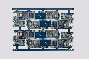
After completing the layout, perform a manufacturability check to ensure that components are not too close to the shielding to prevent short circuits. Also, make sure to maintain a safety margin of 12 mils. Additionally, check whether any components are too close to the board edge, as this could cause them to fall off.
Manufacturability checks for mobile phone circuit boards are commonly referred to as DFM/DFA. For RF circuit boards, there are five additional factors that require special attention:
- Shielding Enclosure Wall Location: No components should be placed below the shielding wall, and soldering clearance must be provided; generally, the wall should be 0.5–0.8 mm wide, with 0.3 mm of clearance on each side.
- Distance from the Device to the Board Edge: Panel separation can cause mechanical stress; it is recommended that components be placed at least 1.0 mm from the board edge, and BGAs and ceramic capacitors should be placed even farther away.
- Pad Spacing: 12 mil (0.3 mm) is the minimum limit; in areas with a high density of RF components, it is easy to come close to the minimum spacing, so a full DRC check is required.
- Via for the bottom ground pad: Verify the number of vias, their diameters, and the solder mask openings to prevent solder paste from being drawn into the vias, which could cause cold solder joints.
- Steel Mesh Aperture: The opening ratio of the heat-dissipating pads on RF devices must be designed according to the specifications; if the openings are too large, the device may lift off the board.
7. Pre-Launch Checklist

| Checklist Items | Standard Requirements | Common Oversights |
|---|---|---|
| Device Packaging | Consistent with the latest version of the specification sheet; the windowing of the bottom pads is correct. | Created the database using the maximum size |
| Antenna Clearance | PIFA ≥ 500 mm², with no copper or components throughout the entire layer of the projected area | I forgot to hollow out the inner layer. |
| Impedance Line | 50 Ω, tolerance ±10%, bottom layer hollowed out | The floor number was left blank or entered incorrectly |
| Land Lease | The layers above and below the sensitive line are ground; the spacing between ground vias is ≤λ/20 | I leased the land but haven't drilled any holes yet. |
| PA Power Supply | For trace widths ≥80 mil, place decoupling capacitors as close as possible. | If the capacitor is placed far away, the lead inductance is high. |
| Power Supply Topology | Star topology, loop-free | An O-ring was formed |
| Shielding Enclosure | No items should be placed against the wall; leave clear space all around. | The device was placed too close to the wall, causing a short circuit. |
| Device to Board Edge | ≥1.0 mm | The BGA is too close to the edge of the board |
| Layer Symmetry | The laminated structure is symmetrical, which prevents warping. | Asymmetrical copper thickness distribution |
| Process Feasibility | Line width, line spacing, and hole diameter are within the board manufacturer's capabilities | Used 2-mil lines, which PCB manufacturers can't produce |
The last point is particularly important—design rules must be within the actual capabilities of the PCB manufacturer, and they should be verified before placing the order.PCB Manufacturing CapabilitiesDouble-check it.

The six most common sources of interference on RF boards, and the corresponding isolation measures:
| Source of Interference | Coupling Paths | Quarantine Measures |
|---|---|---|
| PA Output Harmonics | Electromagnetic Emissions, Power Coupling | Shielding + Separate decoupling for the PA power supply + Low-pass filter added to the output |
| Clock (26 MHz, etc.) | Spatial Radiation, Common-Ground Impedance | Inner-layer traces + top and bottom ground planes + away from the receive chain |
| Power Supply Ripple | Common-Mode Impedance | Star Topology + Separate LDOs for Each Level + Larger Decoupling Capacitors |
| Digital Cable | Spatial Radiation, Interlayer Coupling | RF Layered Configuration + Increased Spacing + Ground Shielding |
| Display / Camera | Spatial radiation, cable radiation | Physical Separation + Shielded Cables + Grounding Measures |
| Charger / USB | Ground-Loop Noise | Ground Splitting + Single-Point Connection + Common-Mode Filtering |
8. Conclusion
The principles for inspecting the RF section layout are crucial for the design of mobile phone PCBs. By carefully inspecting component packages, ensuring proper component placement, verifying trace definitions and routing specifications across all layers, and conducting manufacturability checks, it is possible to ensure that the RF section of a mobile phone is laid out properly, delivers superior performance, and minimizes potential interference issues.
Frequently Asked Questions
1. Why are the design principles for RF circuit layout so important?
The design of the RF section’s layout directly affects a mobile phone’s performance and reliability, particularly in terms of signal transmission. A well-designed layout can prevent interference issues and improve product performance.
2. Why is it necessary to inspect device packaging?
Component package inspection ensures that the component packages on the motherboard meet specification requirements, thereby preventing issues during subsequent layout processes.
3. Why is it necessary to provide special protection for IQ lines and high-frequency signal lines?
IQ lines and high-frequency signal lines are susceptible to interference; special protection measures can ensure their stability and performance.
4. What are star-type and O-type power networks?
A star-type power network is a power distribution configuration in which each power point is connected to a central point. An O-type power network is a ring-shaped power distribution configuration that can form power loops, thereby degrading EMC performance.
5. Why is a manufacturability review necessary?
Manufacturability checks ensure that the layout is not only sound from a design perspective but also feasible in the actual manufacturing process, thereby reducing production issues.
6. Why is there a hollow layer beneath the impedance line?
There are two objectives: First, to increase the dielectric thickness, which allows for wider trace widths while maintaining the same impedance target, resulting in lower loss and more lenient tolerances; second, to block coupling paths with traces on adjacent layers. When cutting out sections, ensure that the correct layer is being cut and clearly mark it on the stack-up diagram—this is one of the areas where errors most commonly occur.
7. How do you determine the spacing for drilling holes in a plot of land?
Use a value of λ/20 based on the highest operating frequency. At 2 GHz, the wavelength is approximately 150 mm (about 75 mm in FR-4), so the via spacing should be ≤3.75 mm; for safety, an engineering practice is to typically use 1–2 mm. If the via spacing is too large, the ground plane becomes ineffective at high frequencies and may even act as a resonant cavity.
8. Why does the PIFA antenna require 500 mm²?
The resonant frequency of a PIFA (Planar Inverted F Antenna) is determined by the radiating area and the positions of the feed point and shorting point. Since the GSM bands (900/1800 MHz) have relatively long wavelengths, to achieve acceptable bandwidth and efficiency, the projected area of the radiating element should generally be no less than 500 mm², and the space directly beneath the projected area must be completely clear; otherwise, the resonance point will shift and efficiency will drop significantly.
9. Why are shielding enclosures commonly used for RF boards?
The internal space of a mobile phone is compact, with the RF, baseband, power supply, camera, and display driver all located within a few centimeters of each other; complete isolation cannot be achieved through layout spacing alone. Shielding enclosures provide the final line of defense by individually enclosing strong radiation sources such as the PA and VCO. The shielding enclosure’s ground connection must be continuous (typically with a ground tab every 2–3 mm), and the length of any gaps must be significantly less than λ/20 at the highest operating frequency.
10. What is the troubleshooting sequence for RF layout issues?
First, test the passive components (use a vector network analyzer to measure link insertion loss and standing wave ratio to confirm that the routing and matching are correct); then test the active components (check output power, EVM, and receive sensitivity); finally, perform the complete system coupling test (TRP/TIS). If insertion loss is too high, it is most likely due to excessively long traces or impedance mismatch; if sensitivity is poor, it is most likely due to interference in the receive path—focus on checking the package ground and shielding. For key points on high-frequency routing, see12 Key Tips for High-Frequency PCB Design and Routing。
Additional Information:Considerations for Via Design in High-Speed PCB Design · Precautions for Routing High-Frequency PCBs · A Guide to Avoiding Pitfalls in RF PCB Design: Reducing Parasitic Signal Interference