

Special attention must be paid to high-density PCB layout; even the slightest oversight can lead to electromagnetic compatibility and interference issues. Here are some practical routing guidelines.
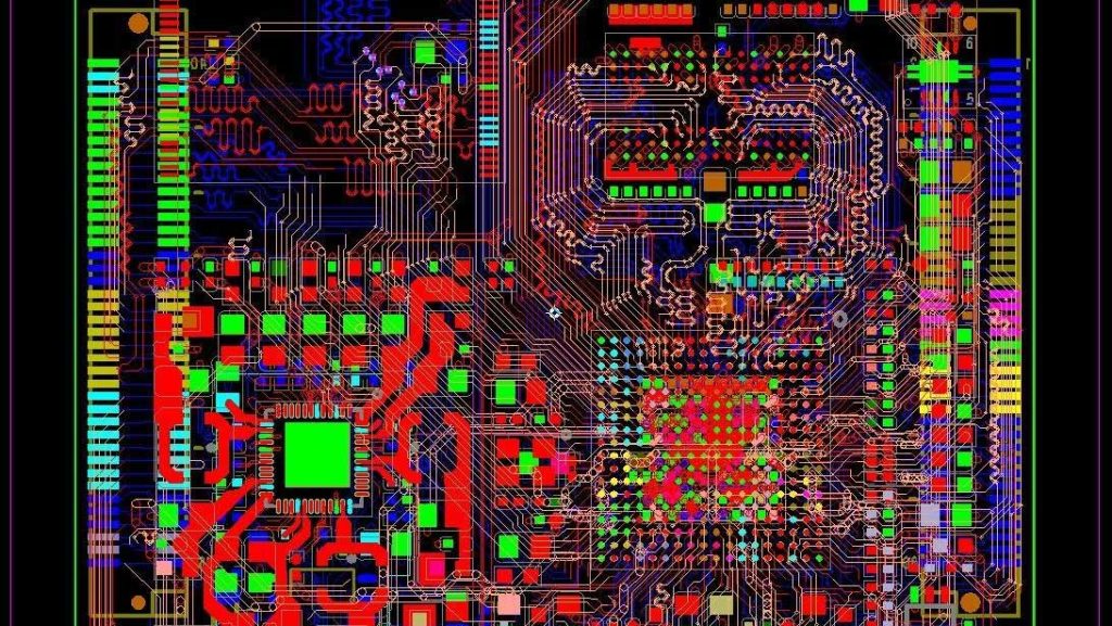
1. The Importance of Wiring
Printed circuit board (PCB) routing plays a critical role in high-speed circuits, but it is often one of the final steps in the circuit design process. High-speed PCB routing involves many complex issues, and a vast amount of literature has been written on this topic. This article explores high-speed circuit routing primarily from a practical perspective. Its main purpose is to help new users become aware of the various issues that need to be considered when designing high-speed circuit PCBs. Another objective is to provide a refresher for customers who have not worked on PCB routing for some time. Due to space limitations, this article cannot cover all issues in detail; however, we will discuss the key areas that are most effective in improving circuit performance, shortening design time, and reducing revision time.
2. A Well-Designed Schematic
Although a well-designed schematic does not guarantee good layout, good layout begins with a well-designed schematic. When drawing a schematic, think carefully and be sure to consider the signal flow throughout the entire circuit. If the signal flow from left to right is normal and stable in the schematic, it should be just as good on the PCB. Include as much useful information as possible on the schematic. Since circuit design engineers are not always available, customers sometimes ask us to help resolve circuit issues. Designers, technicians, and engineers working on these projects—including ourselves—will be very grateful for this.
In addition to standard reference identifiers, power consumption, and tolerance values, what other information should be included in a schematic? Here are some suggestions that can help transform an ordinary schematic into a top-notch one. Include waveforms, mechanical information about the enclosure, trace lengths, and blank areas; indicate which components need to be placed on the PCB; provide adjustment information, component value ranges, thermal management information, controlled-impedance traces, annotations, and a brief description of the circuit’s operation…
3. Carefully inspect the wiring
If you aren’t designing the layout yourself, be sure to set aside ample time to carefully review the layout engineer’s design. In this regard, a little prevention is worth a hundred times the cure. Don’t expect the layout engineer to understand your ideas. It’s crucial to involve the layout engineer early in the process. The more information you provide and the more involved you are throughout the routing process, the better the final PCB will be. Set a tentative completion date for the routing engineer and conduct quick reviews based on progress reports to ensure the routing is proceeding as you intend. This approach prevents the routing from going off track, thereby minimizing the likelihood of rework.
4. The Importance of Location
Just as with PCBs, placement is everything. Where a circuit is placed on the PCB, where its specific components are mounted, and what other circuits are adjacent to it—all of these factors are crucial. Typically, the locations of inputs, outputs, and power supplies are predetermined, but the circuits connecting them require a bit of “creativity.” Start by considering the placement of key components, taking into account both the specific circuit and the PCB as a whole. Defining the positions of key components and signal paths from the outset helps ensure the design meets its intended operational goals. Getting the design right the first time reduces costs and stress, thereby shortening the development cycle.
5. Bypass Power Supply
Bypassing the power supply at the amplifier's power input to reduce noise is a very important aspect of PCB design, whether for high-speed operational amplifiers or other high-speed circuits. There are two common configurations for bypassing high-speed operational amplifiers.
Power-Supply-Side Grounding: This method is the most effective in most cases and involves connecting the operational amplifier’s power supply pin directly to ground using multiple capacitors in parallel. Generally, two capacitors in parallel are sufficient, but adding more parallel capacitors may offer benefits in certain circuits. Connecting capacitors with different capacitance values in parallel helps ensure that the power supply pin experiences only very low AC impedance across a wide frequency range. This is particularly important at the frequency where the operational amplifier’s power supply rejection ratio (PSR) begins to roll off. These capacitors help compensate for the amplifier’s reduced PSR. Maintaining a low-impedance ground path across many decades of frequency will help ensure that harmful noise cannot enter the operational amplifier.
Routing is a critical aspect of PCB design, especially in high-speed circuits. Proper routing ensures circuit performance while minimizing the effects of electromagnetic interference. Therefore, designers and engineers should work closely together and follow the guidelines outlined above to achieve a high-performance PCB layout.
In PCB design, the routing of high-speed circuits is a complex and critical process. Effective routing can improve circuit performance, reduce interference, and thereby ensure product stability and reliability. Through well-thought-out schematics, careful inspection and placement considerations, and effective power bypassing, designers can overcome the challenges of high-speed routing and achieve outstanding results.
Frequently Asked Questions (FAQs)
1. Why is PCB routing so important for high-speed circuits?
PCB routing directly affects the performance and stability of high-speed circuits. Proper routing can reduce signal distortion and electromagnetic interference, ensuring that the circuit operates normally.
2. Why is a well-designed schematic the starting point for good routing?
A schematic provides a blueprint for a circuit; a well-designed schematic guides the routing process and ensures smooth signal flow, thereby achieving optimal performance.
3. Why is placement so critical in wiring?
Placement determines the relative positions of circuit components and affects signal transmission and interference. Proper placement can improve circuit performance.
4. What is a bypass power supply, and why is it important?
A bypass power supply is a technology used to reduce power supply noise, which is particularly critical for high-speed circuits. It ensures that the circuit receives a clean power supply, thereby improving performance.
5. How can electromagnetic interference be avoided?
To avoid electromagnetic interference, proper wiring design is essential, including appropriate layout planning and power bypassing. In addition, shielding and filters can be used to minimize the effects of interference.
The guidelines and FAQs above will help you better understand the importance of high-speed circuit layout and take the appropriate steps to ensure circuit performance and reliability. If you need further guidance or have any other questions, please feel free to contact us.
