

With the rapid development of 5G technology, the demand for electronic devices continues to grow. As a critical component of electronic devices, PCB (Printed Circuit Board) manufacturing technology is also constantly evolving. In the manufacturing of 5G PCBs, the drilling method is one of the most crucial steps, as it directly affects the functionality and quality of the circuit board. In this article, we will provide a detailed overview of the three common drilling methods used in 5G PCBs: through-holes, blind vias, and buried vias.
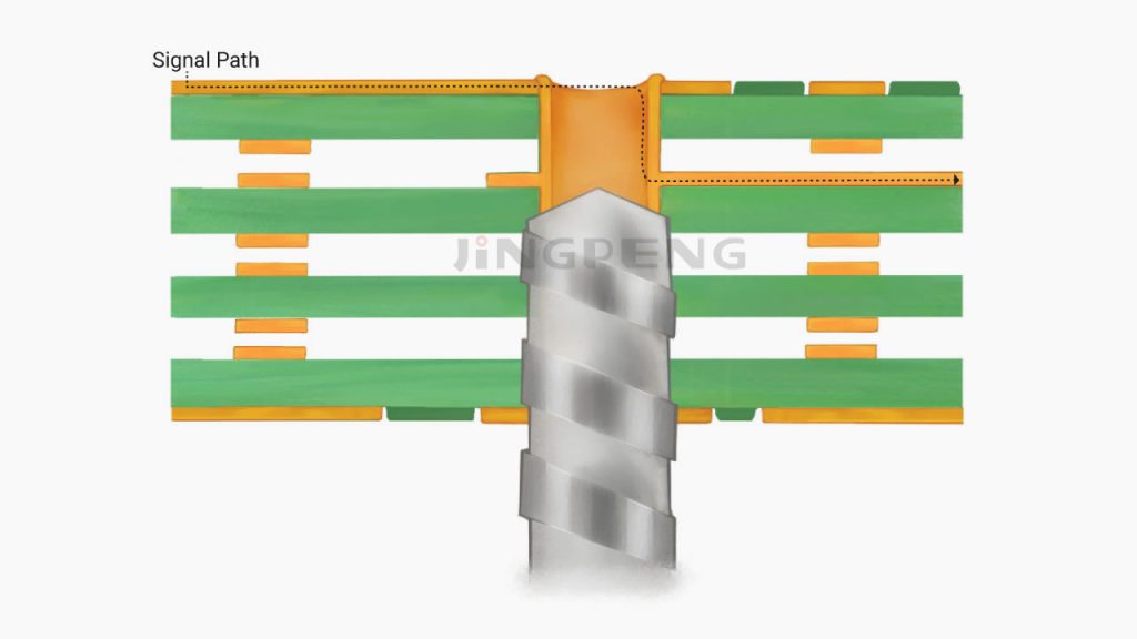
Through-Hole (VIA)
Through-holes, also known as VIAs, are one of the most common types of drill holes. They are used to establish connections between different layers of a circuit board to enable electrical continuity or connect different parts of the board. Unlike other types of holes, through-holes allow signals to flow between different layers, thereby enabling the creation of complex signal paths. In 5G PCBs, where the board typically consists of multiple layers of copper foil stacked on top of one another, through-holes play a particularly important role in ensuring stable signal transmission and connections.
Blind hole
A blind via is a type of drill hole that connects the outer layers to the inner layers of a printed circuit board. Unlike through-holes, blind vias connect only certain layers of the board and are typically located between the top and bottom layers. Because blind vias have a limited depth, they offer unique advantages in achieving high-density routing and saving space. However, manufacturing blind vias requires more precise process control to ensure the quality and consistency of the vias.
Blind Hole
A buried via is a type of hole used to connect different circuit layers; however, it is independent of the outer layers and does not extend to the surface of the PCB. Buried vias are commonly used in situations where connections need to be established between internal layers, such as for signal transmission in multilayer PCBs. The fabrication of buried vias involves complex process steps, including drilling, retreading to the inner layers, and electroplating, which results in higher costs. Buried vias are typically used in high-density circuit boards to optimize space layout and signal transmission.
In the manufacturing process of 5G PCBs, selecting the appropriate drilling method is crucial for ensuring the performance and quality of the circuit board. Through-holes, blind vias, and buried vias are the three common drilling methods, each with its own unique characteristics and applications. Manufacturers, designers, and fabricators need to select the most appropriate drilling method based on actual requirements to meet the signal transmission and connectivity needs of various electronic devices.
Frequently Asked Questions
1. What is the difference between through-holes and blind holes?
Through-holes connect all layers of a circuit board, while blind holes connect only some layers and are typically located between the top and bottom layers of the circuit board.
2. In what situations is blind drilling appropriate?
Buried vias are commonly used in high-density circuit boards where signal connections need to be established between different circuit layers.
3. Does the choice of drilling method affect the cost of the circuit board?
Yes, different drilling methods involve different manufacturing processes, which therefore affect the manufacturing cost of the circuit board.
4. How can we ensure the quality of the drilling?
During the manufacturing process, parameters such as drilling depth and diameter must be strictly controlled to ensure that the quality of the drilled holes meets the requirements.
5. Why are through-holes so important in 5G PCBs?
Due to the complexity of the signal paths in 5G PCBs, through-holes enable signal transmission and connections between different layers, ensuring the performance and stability of the circuit board.
