As a core component of modern electronic devices, PCBs (Printed Circuit Boards) play a crucial role in the electronics industry due to the various manufacturing methods used for their different layers and structures. This article will provide a detailed overview of the components and manufacturing processes of PCBs, including single-layer, double-layer, and multilayer structures, as well as the primary functions of each layer.

Advanced: The Hierarchical Relationship from Raw Materials to Finished Panels
The original text lists the constituent elements, such as pads, vias, and traces. To understand their relationships, you can first look at the hierarchy of a PCB, from raw material to finished product:
| Level | Content | Note |
|---|---|---|
| Raw Materials | Copper-clad laminate (base material + copper foil) | The Basis for Determining Electrical and Thermal Performance |
| Conductive Patterns | Wires, Pads, Fill Areas | Formed by etching copper foil |
| Interconnection Structure | Through-holes, Blind Holes, Buried Holes | Implementing Inter-Layer Connections |
| Protective Layer | Solder Mask, Surface Treatment | Solder mask, oxidation protection, and guaranteed solderability |
| Identification Layer | Screen-printed layer | Component Part Numbers, Polarity, and Version Information |
| Structural Layer | Plate and frame, mounting holes, electrical boundaries | Mechanical Mounting and Installation Range |
| Finished Product | PCBA | Assemblies After Component Placement |
This hierarchical relationship illustrates one thing:The “components” listed in the original text actually belong to different levels and are formed through different manufacturing processes.. The conductors and pads are created through etching; vias are created through drilling and electroplating; screen printing and solder mask application are part of the back-end printing process; and mounting holes and electrical boundaries are part of the structural design. Understanding this allows designers to know at which stage each type of element should be defined.
- Conductive Patterns and Interconnects: Once determined during the design phase, it is difficult to change later;
- Protection and Identification Layer: Can be adjusted as needed before production, with minimal cost;
- Structural Layer: Due to constraints imposed by the housing and assembly, this should be secured first.
- First, define the panel frame, mounting holes, and electrical boundaries;
- Stacking and interconnection schemes;
- Finally, refine the solder mask, screen printing, and process requirements.

For the material system, seePCB Sheets; For components, seeComponent Supply。
I. Components of a PCB
A PCB is a complex assembly that includes multiple important components, each of which has its own unique function:
1. Pad
A pad is a metal hole used for soldering.Componentsthe pins, ensuring they are securely connected to the circuit board.
2. Via
A via is a metal hole used to connect component leads across different layers, enabling signal transmission and electrical connections.
3. Mounting Holes
Mounting holes are used to secure the printed circuit board, ensuring it remains firmly in place within the electronic device.
4. Wires
Traces are the copper patterns on a circuit board that form the electrical network; they are used to connect the pins of components and enable signal transmission.
5. Connectors
Connectors are components used to connect circuit boards, facilitating communication between different circuit boards.
6. Filling
Filling refers to the copper plating used in ground plane networks, which helps reduce impedance and improve circuit performance.
7. Electrical Boundaries
Electrical boundaries are used to define the dimensions of a circuit board and ensure that all components are placed within the specified limits.
Advanced: Key Parameters for Pads and Vias
The original text describes both pads and vias as “metal holes,” but in reality, their functions and parameter systems are completely different:
| Comparison Items | Pad | Via |
|---|---|---|
| Function | Soldered Component Pins | Interlayer Electrical Interconnects |
| Is it welded? | 是 | Usually not welded |
| Key Parameters | Pad Diameter, Hole Diameter, Solder Mask Opening | Pore size, pad ring width, thickness-to-diameter ratio |
| Design Basis | Component Package Dimensions | Current Carrying Capacity, Process Capability, Wiring Density |
| Surface Treatment | Must be covered | Depends on the process (cutting windows, applying a topcoat, plugging holes) |
| Common Defects | Insufficient solder, cold solder joints, missing pads | Insufficient copper in the holes; separation of the hole walls |
In pad design,The annular ring is the parameter most likely to be overlooked.. This refers to the width of the copper ring extending from the hole wall to the outer edge of the pad, which determines whether the connection can be maintained in the event of drilling deviations. According to the general requirements of IPC-6012 Class 2, the minimum width of the hole ring must not be less than 0.05 mm; however, in actual production, designing to this minimum value can easily result in ring breakage or even pad detachment.
- 0.30 mm pore size: Recommended pad size: ≥ 0.60 mm;
- 0.50 mm pore size: Recommended pad size: ≥ 0.80 mm;
- 1.00 mm pore size: The recommended pad size is ≥ 1.40 mm.
Regarding vias,The wall-to-diameter ratio is a hard constraint.: When the board thickness is divided by the hole diameter, the reliable drilling ratio for conventional mechanical drilling is approximately 8:1; when this ratio exceeds 10:1, the uniformity of the copper plating on the hole walls decreases sharply. Therefore, the hole diameter design for high-layer-count PCBs is often not determined by routing requirements, but rather derived by working backward from the board thickness.

For a classification of vias, seeWhat are the different types of PCB vias?; For spacing requirements, seeElectrical Safety Clearances。
Advanced: Design Constraints for Mounting Holes, Connectors, and Electrical Boundaries
The original text also lists these three categories as constituent components. They belong to the structural level, and their constraints stem primarily from assembly rather than electrical considerations:
| Elements | Key Constraints | Common Values |
|---|---|---|
| Mounting Holes | Fastener Specifications, Hole Rings, and No-Place Zones | M2.5: No routing at 3.5 mm; M3: No routing at 4 mm |
| Connectors | Position Determined by Structure; Space for Insertion and Removal | Determine based on the openings in the housing and the routing of the wiring harness |
| Electrical Boundaries | Plate and Frame Dimensions and Wiring Scope | The distance between the wiring and the edge of the board is typically ≥ 1 mm |
| Process Edge | Placement Conveyance and Gripping | 3–5 mm |
| Mark Point | Optical Positioning | 1.0–1.5 mm in diameter, 2–3 |
The no-go zone around mounting holes is often underestimated. Screw heads and washers have actual outer diameters, and tightening tools require operating space; if components are placed too close together, interference will occur during assembly.Setting aside a 3.5 mm / 4 mm exclusion zone, as specified in the original text, is the safest approach with the lowest cost.; If space is limited and adjustments are needed, you should first test-fit the items to confirm they will fit.
- Connectors should be positioned closest to the edge of the panel: Easy to plug in and unplug, and convenient for cable routing;
- Do not run cables within the electrical boundary.: Traces may be cut during panel separation;
- The flash is removed during the molding process.: When designing, make sure to provide a way to remove it.
II. Structure of a PCB
PCB boards typically come in three types: single-layer, double-layer, and multilayer. Here is a brief description of each:
1. Single-Layer PCB
A single-layer board has copper plating on only one side; the other side is not plated. Components are typically mounted on the unplated side, while the plated side is used for routing and soldering.
2. Double-Layer PCB
A double-sided PCB has copper cladding on both sides, typically referred to as the top layer and the bottom layer. Components are usually mounted on the top layer, while the bottom layer is used for soldering the components.
3. Multilayer Printed Circuit Board (PCB)
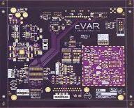
A multilayer board consists of multiple functional layers, including the top layer, the bottom layer, and several intermediate layers. The intermediate layers can serve as conductor layers, signal layers, power layers, ground layers, and so on. Each layer is electrically isolated from the others and connected via vias.
Advanced: A Comparison of Manufacturing Processes and Costs for Three Structures
The original text introduces three types of structures: single-layer, double-layer, and multi-layer. By comparing them in terms of manufacturing processes and costs, the criteria for selection become clearer:
| Dimension | Single-layer board | Double-layer board | Multilayer Board |
|---|---|---|---|
| Copper-clad side | Page 1 | 2 pages | Starting on the 4th floor |
| Interlayer Interconnects | 无 | Through-hole | Through-Holes + Blind/Buried Holes |
| Key Processes | Circuit Lines, Etching, Solder Mask | Add Drilling and Electrolytic Copper Plating | Add an inner layer, laminate, and drill multiple holes |
| Wiring Flexibility | Low; wires must not cross | In, can be crossed | Tall, capable of covering an entire plane |
| Signal Integrity | Poor; no reference plane | Generally | Okay, I have the complete floor plan. |
| Relative Cost | Lowest | Intermediate | Higher, increasing with the number of layers |
| Typical Applications | Adapters, Remote Controls | Home Appliance Control Boards, Industrial Control Boards | Communications equipment, servers |
A practical criterion:Is impedance control required?. If the board includes controlled networks such as USB, Ethernet, HDMI, or DDR, it is difficult to ensure impedance consistency on a double-sided board due to the lack of a complete ground plane; in such cases, a four-layer board should be used instead. This is also the root cause of many issues where “the board powers on normally on a double-sided board but becomes unstable in mass production.”
- Functional Prototype: Double-layer boards are usually sufficient and offer the best balance of cost and lead time;
- Small-batch production: A four-layer board is a safe starting point;
- High-speed or high-density: Six or more stories, or HDI Plan.
- Count the number of networks and BGA pitch to estimate the minimum number of trace layers;
- Determine whether there is a need for impedance control;
- Review the number of layers based on the cost target; if further reduction isn't possible, consider using HDI.
For details on the multi-layer structure, seeCharacteristics of Multilayer Printed Circuit Boards and How They Differ from Double-Sided Boards; For layout rules, see13 Rules for Laying Out Components on Printed Circuit Boards。
III. Operational Aspects of PCBs
PCB boards consist of various types of functional layers, each of which serves a specific purpose:
1. Signal Layer
Signal layers are primarily used for placing components or routing signals. Typically, the top and bottom layers are used for placing components or applying copper, while the intermediate layers are used for routing signals.
2. Protective Layer
Protective layers are used to ensure that areas of the circuit board that do not require tin plating are not accidentally plated, thereby maintaining the board's reliability. These include the solder mask layers on the top and bottom layers, as well as the solder paste protective layer.
3. 丝印层
丝印层主要用于在印刷电路板上标记元器件的流水号、生产编号、公司名称等重要信息。
4. 内部层
内部层主要用作信号布线层,通常存在多个内部层,具体数量取决于设计需求。
5. 其他层
其他层包括钻孔方位层,用于确定印制电路板上钻孔的位置。
以上是PCB线路板的基本组成、结构和工作层面的详细介绍。这些信息有助于您更好地理解PCB线路板的工作原理和制作过程。
进阶:EDA 软件里的层与实物层的对应
原文按功能介绍了信号层、防护层、丝印层、内部层等。在 EDA 软件中,这些「层」有更细分的类型,与实物一一对应:
| EDA 层类型 | 对应实物 | 输出文件 |
|---|---|---|
| Top / Bottom Layer | 顶底层铜箔 | 线路 Gerber |
| Mid Layer | 内层铜箔 | 内层 Gerber |
| Top/Bottom Solder | Solder Mask Cutouts | 阻焊 Gerber |
| Top / Bottom Paste | Steel Mesh Perforations | Steel Mesh Documents |
| Top / Bottom Overlay | Screen-printed layer | 丝印 Gerber |
| Drill Drawing / NC Drill | 钻孔位置与尺寸 | Drilling Documentation |
| Mechanical / Keep-Out | 板框与禁布区 | 外形 Gerber |
| Multi-Layer | 贯穿各层的焊盘 | 体现在各层 |
输出 Gerber 时最常见的错误是漏层或层类型选错,尤其是阻焊层与钢网层容易混淆:阻焊层决定哪里不盖油,钢网层决定哪里上锡膏,两者用途完全不同,弄反会直接导致焊接问题。
- 输出后要用 Gerber 查看器逐层核对:确认层数、极性与孔径表完整;
- 钻孔文件要单独确认:区分镀通孔与非镀通孔;
- 特殊要求要写在工艺说明里:如阻抗、塞孔、金手指斜边。
- 按上表逐层导出并检查;
- 用查看器模拟叠层,确认对位一致;
- 附上工艺要求文档一起提交。
See Halogen-Free ProcessManufacturing Process for Halogen-Free PCBs;贴装头见Components and Functions of an SMT Placement Head。
独家FAQ
什么是PCB线路板?
PCB线路板是印制电路板的简称,用于连接和支持电子元件,实现电子设备的功能。
PCB线路板的主要组成部分是什么?
PCB线路板包括焊盘、过孔、安装孔、导线、元器件、接插件、填充、电气边界等多个组成部分。
PCB线路板有哪些不同的结构?
PCB线路板的结构有单层板、双层板和多层板三种。
多层板中的工作层面有什么作用?
多层板中的工作层面包括信号层、防护层、丝印层、内部层等,各自具有不同的功能,用于支持电路板的正常运行。
什么是填充区(敷铜)?它有什么作用?
填充区是在板面空白区域铺满铜箔的区域,通常连接到地网络。它的作用有三个:为信号提供低阻抗回流路径、降低地阻抗并改善屏蔽效果、以及均衡各层的铜分布以避免蚀刻不均与板面皱折。铺铜后需要打足够的地过孔,否则可能变成浮动导体反而成为干扰源。
焊盘和过孔可以合用吗?
可以,但要看情况。在密度极高的设计中,有时会把过孔直接做在焊盘上(Via-in-Pad),前提是必须做树脂塞孔加电镀盖帽,否则回流时锡膏会被吸入孔内造成少锡。这种做法成本较高,一般只在 BGA 间距极小时才采用。
电气边界和板框有什么区别?
电气边界(Keep-Out)定义的是允许布线与放置元件的范围,板框(Board Outline)定义的是板子的实际外形。两者通常相近但不重合:布线需要距板边留出一定余量,因此电气边界一般比板框内缩 1 mm 左右,以避免分板时切到走线。
丝印层会影响电气性能吗?
正常情况下不会,丝印是非导电的油墨层。但若丝印覆盖到焊盘上,会阻碍焊接导致上锡不良;若丝印压在过孔上,也可能影响测试点的接触。因此设计规范要求丝印避开焊盘与测试点,这也是工厂在投板前会检查的项目之一。
阻焊层和钢网层为什么会弄混?
因为两者在 EDA 里都表现为「开口」图形,视觉上相似。区别在于阻焊层(Solder Mask)的开口表示此处不盖阻焊油墨、露出铜;钢网层(Paste Mask)的开口表示此处要印刷锡膏。阻焊层用于电路板制造,钢网层用于制作 SMT 钢网,用途完全不同。
多层板的中间层一定是布线层吗?
不一定。中间层可以用作信号布线层,也可以作为电源层或地层(通常为大面积铜箔)。在高速设计中,通常优先把中间层安排为平面层,为相邻的信号层提供参考平面与回流路径,这对信号完整性的帮助远大于多一个布线层。
为什么安装孔周围要设禁布区?
因为紧固件有实际外径,垫圈与拧紧工具也需要操作空间。若元件或走线离孔太近,装配时会发生干涉,螺钉头部还可能压到元件造成损坏。原文之外补充一点:金属螺钉与走线之间还需考虑电气间隙,高压产品要按耐压要求单独核算。
一块板上可以同时有单面和双面贴装吗?
可以,这就是双面贴装。需要注意第二次回流时第一次焊好的元件会再次经历高温,重元件可能掉落,因此通常把重元件安排在后焊接的一面。双面贴装能显著提高密度,代价是工序增加、成本上升,且底面元件需避开波峰焊接触区。
Further Reading:Components and Functions of an SMT Placement Head · Manufacturing Process for Halogen-Free PCBs