

In the PCB manufacturing process, there are generally three methods for treating vias: opening windows, covering with solder mask, and filling with solder mask. So, what is via solder mask coverage, and what is the difference between solder mask coverage and filling with solder mask?
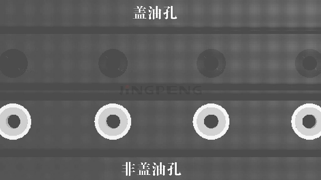
1. Definitions of Terms Related to Bore Cover Oil
"Via plating" refers to ensuring the proper ink thickness on the via ring; the key control points are preventing pseudo-copper exposure on the ring and ensuring the ink is not too thin at the via opening.
2. What is via cover coating in PCB manufacturing?
- When sending your files (in PADS or ProTel format) to the factory and requesting solder mask coverage for vias, be very careful to check whether your through-hole pads also use vias. Otherwise, solder mask will be applied to your through-hole pads as well, preventing soldering. Point of contention: Surface-mount pads are definitely meant to be tinned—why would you cover them with solder mask? How am I supposed to use them? Before you say that, please check your files to see if they were designed as pads or vias!
- When you send your files to the factory in PADS or Protel format and place an order specifying “via filling,” many customers use pads (through-hole pads) to represent conductive vias, which can result in your conductive vias being left open. If you actually want the vias filled, a potential point of contention later on might be: “I specifically asked for the vias to be filled—why were they left open?” In that case, please double-check your file design!
3. The Difference Between Via Filling and Via Plugging
The requirement for via plating is that the ring around the through-hole must be covered with ink, with particular emphasis on the degree of ink coverage at the hole edges. Examples include pseudo-copper exposure or a reddish tint around the hole edges.
Via filling refers to the process of filling the interior of a through-hole with ink, with an emphasis on the quality of the filling. For example, light should pass through the via after it has been filled.
4. Understanding the Difference Between Via Plating and Via Filling in PCB Manufacturing
To fill via holes with ink, first completely fill the entire via hole with ink to seal it off. This prevents the ink from the solder mask from flowing into the via hole, thereby preventing the via holes from turning yellow. (If you have strict requirements and have ordered via hole ink filling, and you notice that the ink filling is not sufficiently full or has a yellowish tint, you can switch to the “via filling” method later on). Additionally, the smaller the via, the easier it is to fill; therefore, the vias to be filled should not be too large.
In PCB manufacturing, the method used to process vias is extremely important, as different methods serve different purposes and have different requirements. Selecting the appropriate processing method ensures the quality of the vias, thereby improving the reliability and performance of the circuit board.
5. Frequently Asked Questions
Q1: What is via fill?
A1: "Via plating" refers to ensuring the required ink thickness on the via ring; the key control points are preventing pseudo-copper exposure on the ring and ensuring the ink is not too thin at the via opening.
Q2: How can you tell the difference between filling vias with solder paste and plugging vias?
A2: "Via plating" refers to the degree of ink coverage around the edges of the vias, while "via filling" refers to the quality inside the vias—such as whether light shines through after the vias have been filled.
Q3: How do I choose the right via treatment method?
A3: The choice of via processing method should be determined based on product requirements and design specifications to ensure that the appropriate method is selected to guarantee PCB quality.
