

In today’s technology-driven world, the design and development of electronic products are critical processes, and the PCB (Printed Circuit Board) design phase is particularly crucial. This article will outline the key steps in electronic product design, with a focus on important considerations and guidelines for the PCB design process.
Preliminary Production Design: Key Steps and Importance
The first step in electronic product design is preliminary production design, which differs from a proof-of-concept (POC) prototype. Preliminary production design focuses on component manufacturing, cost, profit margins, performance, functionality, development feasibility, and manufacturability. At this stage, the cost of each project can be estimated to ensure that the development process is affordable and profitable.
Developing a System Block Diagram: Laying the Foundation for Design
When creating a preliminary production design, the first task is to develop a system-level block diagram. This diagram provides a detailed overview of the electronic functions and how the functional components are interconnected. Using the system block diagram, you can accurately determine the type and number of serial ports required, thereby laying the foundation for selecting the appropriate microcontroller.
Selecting Production Components: The Building Blocks of Electronic Systems
Next, you’ll need to select the appropriate components—such as microchips, sensors, displays, and connectors—based on the product’s features and target retail price. You can then create a preliminary bill of materials (BOM), which is a critical step in the development process.
Estimating Production Costs: Feasibility Analysis
During the preliminary production design phase, it is crucial to estimate the product’s production costs. This helps determine the unit manufacturing cost, which in turn allows for the determination of the optimal selling price, inventory costs, and expected profits. At the same time, it is necessary to consider costs associated with PCB assembly, product testing, retail packaging, logistics, and other factors.
Designing Circuit Schematics: Turning Concepts into Reality
Building on previous work, we can now design a circuit schematic to translate the concept into a concrete circuit layout. The schematic illustrates how the various components are connected, ensuring that the pin numbers for each component are correct. This step requires the use of specific electronic design software.
Designing Printed Circuit Boards (PCBs): The Link That Connects Components
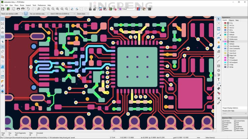
Once you have the circuit schematic, the next step is to design the printed circuit board (PCB). The PCB serves as the physical platform that connects and supports all electronic components; it is the backbone of the entire electronic system. In PCB design, it is essential to ensure that all components are properly laid out and connected.
Key Factors in PCB Layout
When designing a PCB layout, it is important to consider key factors such as power supply routing, high-speed signals (such as crystal clocks and address/data lines), and wireless circuits. A well-designed PCB layout is particularly crucial for products that require a power supply or wireless connectivity. In addition, it is essential to follow the design rules of the PCB manufacturing process to ensure that the PCB matches the schematic.
The PCB design process in electronics design is a critical step in ensuring product performance and reliability. Through preliminary production design, system block diagrams, component selection, cost estimates, circuit schematics, and PCB layout, you can effectively transform a concept into a manufacturable product.
Frequently Asked Questions
1. What is preliminary production design? Preliminary production design is a critical phase in the development of electronic products. It focuses on aspects such as cost, performance, and feasibility, laying the foundation for subsequent development.
2. Why are system block diagrams important? The system block diagram defines the connections between electronic functions and functional components, providing guidance and a foundation for the entire design.
3. How do you estimate production costs? Estimating production costs covers expenses related to manufacturing, assembly, testing, packaging, logistics, and other areas, and helps determine a product’s selling price and profitability.
4. What is the difference between a circuit schematic and a PCB? A circuit diagram shows how electronic components are connected, while a PCB is the physical platform that connects and supports those components.
5. What are the key factors in PCB layout? In PCB layout, key factors include power distribution, high-speed signals, and wireless circuits; it is important to ensure that the routing is reasonable and compliant with PCB manufacturing processes.
