

Anyone who has designed PCBs knows that the design of PCB vias is actually quite intricate. So, what techniques are involved in PCB via design? Today, we’ll share some technical knowledge about vias and back drilling in PCBs with Shenzhen PCB manufacturers.
Via Design in High-Speed PCBs
In high-speed PCB design, multilayer PCBs are often required, and vias are a critical factor in multilayer PCB design.
The Impact of Vias in High-Speed PCBs
In high-speed multilayer PCBs, signals are transmitted from interconnects on one layer to interconnects on another layer via vias. At frequencies below 1 GHz, vias provide an effective connection, and their parasitic capacitance and inductance can be neglected.
When the frequency exceeds 1 GHz, the impact of via parasitic effects on signal integrity can no longer be ignored. At this point, vias act as points of impedance discontinuity along the transmission path, causing signal integrity issues such as signal reflection, delay, and attenuation.
When a signal is transmitted to another layer through a via, the reference layer of the signal trace also serves as the return path for the via signal, and the return current flows between the reference layers via capacitive coupling, causing issues such as ground bounce.
Types of Via Holes
Vias are generally classified into three types: through-holes, blind vias, and buried vias.
Blind hole: Refers to holes located on the top and bottom surfaces of a printed circuit board that have a certain depth and are used to connect the surface-level traces to the underlying internal traces; the depth of the holes typically does not exceed a certain ratio relative to their diameter.
Blind Hole: Refers to a via located within the inner layers of a printed circuit board that does not extend to the board's surface.
Through-hole: These holes pass through the entire circuit board and can be used for internal interconnections or as mounting and positioning holes for components. Since through-holes are easier to manufacture and less expensive, they are commonly used in printed circuit boards.
Via Design in High-Speed PCBs
In high-speed PCB design, vias—which may seem simple—can often have significant negative effects on circuit design. To minimize the adverse effects caused by parasitic effects in vias, the following measures should be taken during the design process:
-
-
- Selecting an Appropriate Via Size: For multi-layer PCB designs of general density, it is best to use 0.25 mm, 0.51 mm, or 0.91 mm (for drill holes, pads, and power isolation zones) for vias; For some high-density PCBs, 0.20 mm, 0.46 mm, and 0.86 mm vias can also be used, or non-through-holes can be considered; for power or ground vias, larger sizes should be considered to reduce impedance;
- The larger the POWER isolation zone, the better: When considering the via density on a PCB, the general rule is D1 = D2 + 0.41;
- Minimize the number of vias: Signal traces on the PCB should remain on the same layer as much as possible; in other words, the number of vias should be minimized;
- Use a thinner PCB: Two parasitic parameters that help reduce via size;
- Nearby Via: The power and ground pins should be routed through vias as close as possible; the shorter the traces between the vias and the pins, the better, because longer traces increase inductance. At the same time, the power and ground traces should be as wide as possible to reduce impedance;
- Ground Via: Place some ground vias near the signal vias where signal layers change to provide a short-distance return path for the signal.
-
In addition, via length is one of the primary factors affecting via inductance. For vias used to connect the top and bottom layers, the via length is equal to the PCB thickness; as the number of PCB layers continues to increase, the PCB thickness often exceeds 5 mm. However, in high-speed PCB design, to minimize problems caused by vias, their length is generally kept within 2.0 mm. For vias longer than 2.0 mm, increasing the via diameter can improve impedance continuity to a certain extent. When the via length is 1.0 mm or less, the optimal via diameter is 0.20 mm to 0.30 mm.
The Back Drilling Process in PCB Manufacturing
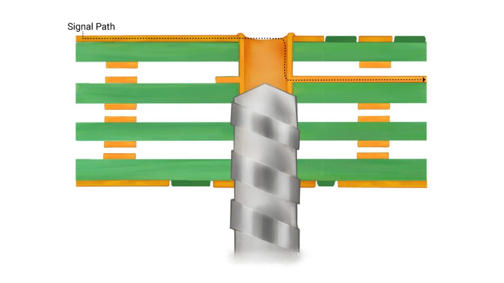
Back drilling is actually a special type of depth-controlled drilling. In the manufacturing of multilayer boards—such as a 12-layer board—we need to connect Layer 1 to Layer 9. Typically, we drill through-holes (in a single pass) and then perform copper plating. This connects Layer 1 directly to Layer 12, but in reality, we only need Layer 1 to be connected to Layer 9. Since there are no circuits connecting Layers 10 through 12, they act like pillars.
This pillar obstructs the signal path and causes signal integrity issues in communication signals. Therefore, this excess pillar (known in the industry as a “stub”) is drilled out from the back side (secondary drilling). This process is called “back drilling,” but the drilling is generally not done completely cleanly, because subsequent processes will remove some copper through electrolysis, and the drill bit itself is pointed. Consequently, PCB manufacturers leave a small portion of the stub intact; the length of this remaining stub is referred to as the “B value,” which is generally best kept within the range of 50–150 µm.
What are the advantages of back drilling?
1) Reduce noise interference;
2) Improve signal integrity;
3) Localized reduction in plate thickness;
4) Reduce the use of blind vias to simplify PCB manufacturing.
What is the purpose of back drilling?
The purpose of back drilling is to remove sections of through-holes that serve no connection or transmission function, thereby preventing reflections, scattering, and delays in high-speed signal transmission that can cause “distortion” in the signal. Research has shown that: In addition to factors such as design, board material, transmission lines, connectors, and chip packaging, through-holes have a significant impact on the signal integrity of a signal system.
How Back-Drilling Works
When drilling with a drill bit, the system detects the height of the board surface by sensing the microcurrent generated when the tip of the drill bit contacts the copper foil on the board surface. It then drills to the preset depth and stops once that depth is reached.
What is the manufacturing process for back-drilled products?
a. Provide a PCB with alignment holes; use these alignment holes to position the PCB and drill a single hole;
b. Electroplate the PCB after single-drill hole drilling; prior to electroplating, apply a dry film to seal the positioning holes;
c. Create the outer layer patterns on the PCB after electroplating;
d. Perform pattern plating on the PCB after the outer layer pattern has been formed; prior to pattern plating, seal the alignment holes using a dry film;
e. Use the pilot holes created by the first drill to position the back drilling, and use a drill bit to perform back drilling on the plated holes that require it;
f. After back drilling, flush the back drill holes with water to remove any remaining drill cuttings.
What are the technical features of back-drilled perforated panels?
1) Most back panels are rigid boards
2) The number of stories is generally between 8 and 50.
3) Sheet thickness: 2.5 mm or greater
4) The wall-to-diameter ratio is relatively high
5) The panels are large
6) Generally, the minimum hole diameter for the first drill hole is ≥ 0.3 mm
7) The outer layers have fewer traces and are mostly designed as arrays of crimp holes.
8) Back-drilled holes are typically 0.2 mm larger than the holes to be drilled.
9) Back-drill depth tolerance: ±0.05 mm
10) If back drilling is required to reach layer M, the thickness of the dielectric material between layer M and layer M-1 (the layer below layer M) must be at least 0.17 mm.
In which fields are back-drilled panels primarily used?
Backplanes are primarily used in telecommunications equipment, large-scale servers, medical electronics, the military, and aerospace sectors. Because the military and aerospace sectors are sensitive industries, domestic backplanes are typically supplied by research institutes and R&D centers affiliated with the military and aerospace systems, or by PCB manufacturers with strong military and aerospace backgrounds. In China, demand for backplanes comes mainly from the telecommunications industry, specifically the rapidly growing telecommunications equipment manufacturing sector.
