

Data Communication PCBs | From End-to-End Channel Budget to Layer Stacking and Vias
High-speed interconnections between switches, servers, expansion cards, and optical modules require the evaluation of traces, vias, connectors, and device ports as a complete channel. Shenzhen Jingpeng Electronics conducts manufacturing reviews focused on stacking, low-loss materials, fan-out, and via structures to define manufacturable geometries and verification criteria.
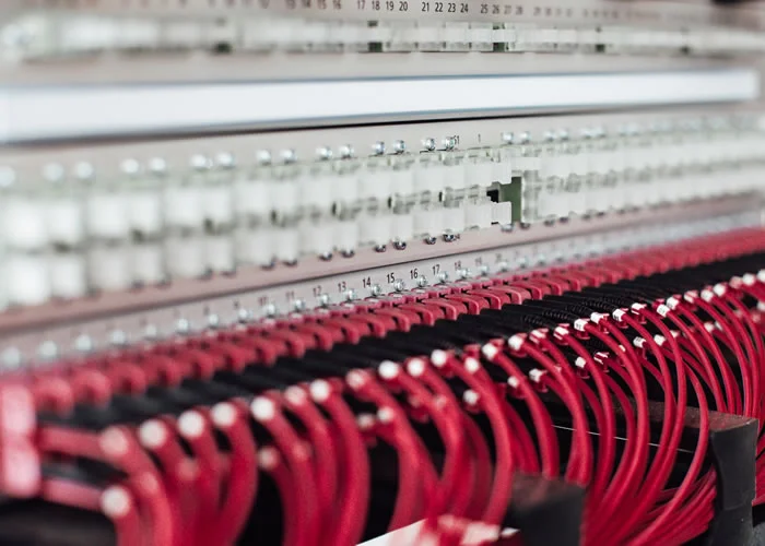
Exhibits Related to Networks and Data Communications | The specific scope of application will be determined on a project-by-project basis.
Divide a passageway into three sections, then reallocate the budget
Do not treat “support for a certain data rate” as a standalone PCB specification. Manufacturing requirements for the same interface can vary significantly depending on channel length and topology.
01
Chip Tracing and Via Placement
Check the BGA area for short circuits, pads, and connections between layers and the reference plane. Dense fan-out may cause localized impedance variations; first clarify the topology and manufacturable dimensions before considering material upgrades.
02
On-Board Tracing and Connection Transitions
Calculate or simulate losses based on length, layer, and material, while taking connectors and vias into account. When allocating the budget, account for the impact of ports and assembly; do not reserve all the margin for long traces within the board.
03
Receiver and System Verification
Device equalization, firmware configuration, and test conditions can affect the final link results. Manufacturing output is used to support verification, but end-to-end criteria must be defined in collaboration with the systems team.
Switches, servers, and optical modules face different layout challenges.
Organize the review materials by major bottlenecks, and avoid using the same high-speed PCB parameter sheet.
Switches and Network Interface Cards
Dense, high-speed ports are concentrated around large packages, requiring a balance between routing, the number of vias, connector placement, and the number of layers. Focus on the most congested areas and the longest paths, rather than just the overall board size.
Servers and Acceleration Cards
High-speed interfaces share layer resources with high-current power networks; check the power plane, decoupling connections, and local temperature rise, while verifying board thickness and connector assembly constraints.
Backplane and Inter-Board Connections
Long vias, multiple connectors, and thick-board vias increase design complexity. Via stubs and connection transitions must be taken into account, and the method of interlayer connection must be determined before selecting materials.
Optical Modules and Compact Subassemblies
With space, thermal considerations, and connector geometries all becoming increasingly constrained, it is essential to distinguish between high-speed signal areas, power supply circuits, and monitoring circuits. The complete signal path after the daughter board is mounted on the motherboard is the subject of system verification.

Images related to applications and manufacturing are used solely to illustrate the scenarios.
Stump Remnants, Backflow, and Fiberglass: Three Issues Often Omitted from Drawings
The following are the criteria for channel evaluation; no upper limits on line width, residual pile height, or spacing are specified for all interfaces.
Borehole Remnants: Described Using a Layer Connection Table
Portions of through-holes that are not involved in signal transmission may affect high-speed signals. First, list the layers through which signals enter and exit, then evaluate options such as changing the routing layers, using blind vias, or back-drilling; different approaches will affect manufacturing and verification costs.
Back-to-Back Drills: From “What’s Needed” to “How to Test It”
Confirm the entry surface, the target layer that must not be touched, permitted residual piles, and surrounding clearance, and agree on the verification method. Back drilling has depth control and alignment limits; do not simply list a process name in the remarks section.
Reflow: A Combined Look at Plane Segmentation and Layer Switching
When a high-speed route crosses a planar gap or changes layers, it is necessary to evaluate whether the reference connection is continuous. Simply matching the geometric lengths of two differential pairs is not sufficient to address all return-path and common-mode issues.
The Fiberglass Effect: Consider Electrical Delay, Not Just Length
The distribution of the dielectric within the material may result in different propagation conditions on either side of the differential pair. Whether specific routing angles, material structures, or other measures are required should be evaluated based on the actual channel length and tolerance.
Link Edge Failure: First, determine which layer the problem belongs to
This is an example of an engineering review and does not correspond to any specific customer product or API capability commitment.
The continuity test passed, but the link is still abnormal.
First, identify the board number, components, firmware, data rate, and test connections; after ruling out issues with connections and power supply, compare the circuit paths with the reference board. A pass on a bare-board continuity test only confirms connectivity within the scope of that test.
Distinguishing Between Geometric Discontinuities and Distribution Losses
Local variations can be identified using TDR or similar methods under agreed-upon test conditions, and channel performance can be analyzed using frequency-domain or system testing; the results from both types of testing must be interpreted in conjunction with the test fixture and reference surface—a single eye diagram alone is not sufficient to determine that the substrate is nonconforming.
When making comparative changes, control the variables.
If changes are made to the material, laminate, and back drilling all at the same time, it is difficult to determine which factor contributed to the improvement. First, establish a baseline; then, modify one or a few related factors according to the approved plan, and maintain the corresponding manufacturing and testing records.
Select processes based on channel bottlenecks; do not configure based on rate-labeled stacks
Refer to the following panel types and process inlets to further verify the specific structure, drawings, and acceptance requirements.
HDI PCB
Re-evaluate HDI when BGA fan-out is constrained by pads, via diameters, and routing channels; clarify requirements for interlayer microvias, lamination sequence, and key verification criteria—complex via structures do not necessarily result in unconditional performance improvements.
PCB Materials
When selecting materials, compare dielectric loss, copper foil, thickness, and availability within the same structure; short channels and long backplanes should not be specified to use the same material simply because their interface names are the same.
PCB Vias
Via layouts must be verified against the actual interlayer connections, checking for stubs, pads, and reflow vias; if back drilling is required, the drilling direction, target layer, and allowable residue must be reviewed separately.
PCB Manufacturing Capabilities
When designing multi-layer stacks, consideration must be given to the reference plane, power supply, thickness, and interlayer connections; provide a table of key layer pairs and their impedances so that manufacturing adjustments can be verified against the original design assumptions.
PCBA Manufacturing Capabilities
High-density BGAs, connectors, and components with high thermal mass can affect placement, soldering, and rework; plan for inspection and jig access during the design phase to avoid having to rely solely on guesswork regarding the condition of solder joints later on.
PCBA Testing
High-speed interface testing requires defining the data rate, bit patterns, firmware, channels, and pass/fail criteria; continuity, impedance, eye diagram, and bit error rate tests each address different issues.
High-Speed Board Input Package: Key Information Beyond Gerber Files
Impedance meters, via connection meters, and test requirements should be associated with the same version of the laminate.
Pathways and Goals
Interfaces and operating modes, end-to-end topology, longest and critical paths, connector models, loss or other acceptance criteria, and their reference conditions.
Lamination and Pore Table
The functions, media, and copper foil of each layer; the impedance network; the layer-to-layer transition structure; requirements for blind vias or back-drilled vias; and the boundaries of adjustments permitted by the engineering specifications.
Delivery and Re-inspection
Test strip structure, reporting requirements, and the division of labor for assembly and system testing; channels that require re-validation following material or stack substitution.
Data Communication PCBs: Answers to Specific Questions
Can a lower Df solve all high-speed link problems?
You should also inspect the copper foil, vias, connectors, reflow, and ports. Upgrading materials can reduce some losses, but it does not automatically fix local discontinuities or assembly issues.
Do all high-speed vias require back drilling?
This depends on the hole connections, residual pile length, and channel tolerances; the decision should be based on the model or verification results. For back drilling, the surrounding routing and manufacturing boundaries must also be reviewed.
Why can there still be a time difference even when the lengths are geometrically equal?
Propagation delay depends on the medium, layer position, and transition structures. Equal length is one of the design constraints and must be verified in conjunction with the full-channel conditions.
The reference materials are intended to help you understand the relevant technical principles; specific parameters and applicable conditions are subject to the project documentation and the corresponding device and material specifications.
TI: PCB Layout Guidelines for High-Speed InterfacesRF and Antennas: Explore Communications ApplicationsEvaluate high-speed board manufacturing solutions using channel topology
Please provide the key interfaces, trace lengths, connector and via topologies, stack-up, and loss budget. Shenzhen Jingpeng Electronics will work with you to confirm the materials, via structures, tolerances, and the verification records that need to be retained.
